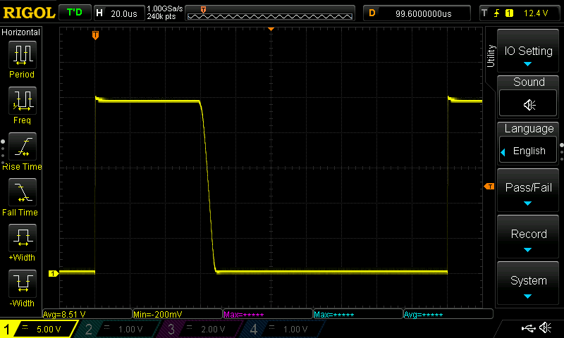
swapped out R57, gave me a super clean signal out, doesn’t change anything on the output though. following the signal through the FETs, I clearly do not understand what is happening. I send in a pwm signal and the first one spits out something odd, almost an inverse, then the second one spits out a pwm signal again. so crazy.
Not almost inverse, inverse (within the limits of behavior of the Q8 FET itself.).
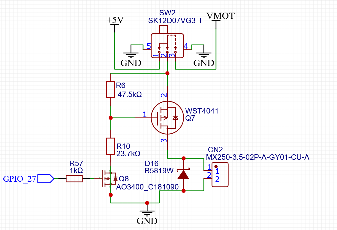
The Q7 FET’s gate has to be pulled LOW to turn it on, so when you turn on Q8 you are pulling the gate of Q7 LOW, by tying it through Q8 to GND. Now that you’ve turned on Q7, it’s output on Pin 3 goes high to whatever you gave it on pin 2. Notice that the little arrow in the symbol for the FET points in the opposite direction, this is how you can tell if your device is N channel or P channel.
Had to try it at 24v, , rise time looks way better than the fall time still. The larger resistor on the gpio pin make that fall time much better. maybe I went the wrong way. the 1k-2.2k made the fall time better.
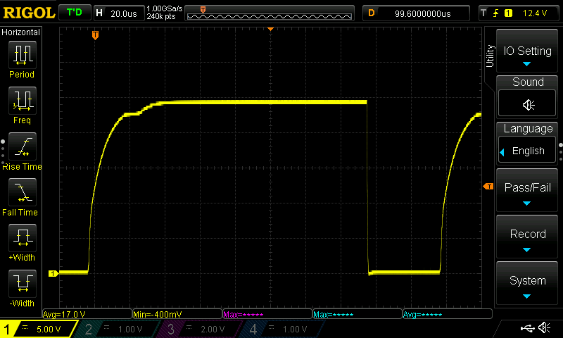
well, the rise time of the first inverse is horrible, completely rounded corner. I guess I will focus on this first FET then.
Yep. That’s all the detail Jono went through up above quoting semiconductor theory. This circuit as it currently is does not do fast switching well. (The Jackpot V1 circuit, however, does.)
I’m not sure what one could do to make this flexible voltage select design work for a fast PWM signal, which is why I keep saying you need a design EE not a test monkey like me to thourougly sort it out.
You’re making really good progress, though. When I start talking electrons most of the Mech Es near me at work flee.
The issue here is the selectable voltage. The jp1 forces the output to either 5v highside or 24V low side switch. This was designed to let us chose 5v or 24v high side switching. So it means two mosfets instead of one, one to switch the switch and the other switch choses the voltage. What I am learning is the lag is more than I thought.
I could but they are very busy so he may or may not have time. I try to only bug them if it is firmware related, since his time is better spent there.
Not sure yet. I assume we can, but I am really hoping we can get this just a bit faster and be okay, at least for this batch of boards. Then figure out what to do with the next ones.
That’s exactly it. It’s a mildly inaccurate voltage measurement plotted vs very accurate time. Compared to the voltage range of a multimeter which is quite accurate voltage but the time part is kinda ‘now, ish, with a bit of averaging’.
There’s 3 we’re talking about. At the moment when the output MOSFET (just a switch, really) turns on, it connects pin 1 of CN2 to +V, but there’s nothing that forces that same pin to 0V when it turns off, so if there’s any capacitance there (which there always is), it’ll stay at +V for a while until it slowly drops. Adding a resistor to ‘pull down’ that voltage is one way to help that, which is just connecting a resistor directly between pin 1 and pin 2 of CN2. The other 2 resistors are R10 and R6. There needs to be 2 resistors there because the only options for controlling the gate on Q7 is Q8, which can only be on or off. If Q8 is off then R6 pulls the gate up to the same voltage as the source on the MOSFET, turning it off. If Q8 is on then it pulls one side of R10 to 0V. If there was no R10 and it was just a direct connection, the gate-to-source voltage would be the same as the supply voltage. The FET can only handle 20V so if we used it with a 24V supply, that’d get damaged. So R10 and R6 create a voltage divider meaning the gate will always be in a ‘safe’ voltage range, even when used with +24V.
I was just looking at the numbers on your gate dividers and I’d be changing the ratio on those a bit, at 5V you’re not really turning the FET on very hard at all, I’d be getting a little nervous of that. Vgs(th) can change over time and it’s often poorly specified, 3.3V on the gate is pretty low. That’s always going to be a bit awkward with that approach and I could see that Q7 burning if used for anything significant at 5V. Personally I hate high-side switching for tricky issues like that so I’d usually use something like a dedicated high-side driver IC for that process, or low-side switching. Is there a particular reason you’ve gone for the high-side switching here?
A near-term solution may be to clamp Vgs with a zener instead of just using the divider. It’ll be less efficient but will solve that particular problem.
Bear in mind that Q7 doesn’t switch on from 0 to -5V on the gate, it starts switching from off to on at Vgs(th) which is -0.8V to -2.2V and then is probably turned on completely by the time another volt is added (well, removed in the case of the P channel). So your important part of the gate waveform isn’t the whole thing, it’s maybe -1.5V to -2.5V, that’s the bit you need to be fast.
It’s always difficult to make things generic and flexible. If all you want is something that’ll control a motor, FAN or lighting then this is adequate. If you want something that’ll control a PWM then you’d be better off in other ways.
At this point, I’d take a step back and think about requirements. That’s always where this stuff should start. How fast do you need? As Jim said above, hundreds of kHz for a power supply is different to single digit kHz for a laser control. How accurate does it need to be, as well? 5kHz and 10% accurate would be around 10us fall time. 50kHz and 1% accurate would be 100ns fall time. Can it be even slower, like 500Hz? If movement is happening at 50mm/s then that’s 1 pulse every 0.1mm which might be below the spot size of the laser?
There’s also always the option of just saying ‘no, this can’t do that’ and if someone needs it you can wire directly off the drain of Q8 and jumper that to the output. That’d give you a faster option, potentially.
I assume you mean change the divider so it applies more voltage to the gate? That will work because your critical point is the -1V to -4V range, so given that you’ll always get that same RC time constant shape, having it end at a higher voltage means you’re transitioning through the 1-4V range faster. The downside there is that you’ll lose the ability to work at 24V without blowing up the gate on your FET. The compromise there could be a zener tacked across R6 to limit Vgs to ~15V or so but that needs some care because the zener will then be dissipating some power which means R6 needs to be sized carefully as it will have potentially 9-10V across it. Not impossible, but it’d be easy to make it a bit ugly.
Edit: Sorry for bombing the thread with so many responses, trying to catch up with the 32 replies that occurred while I was asleep!
Low side was getting some complaints on the 24v jp1 so I just went for both high side.
I honestly did not think about the lasers at all.
So maybe one 5V pwm and the other two switched as is, is a good compromise. I love the idea of all three the same but that is looking not feasable.
still fuzzy here. I am finding specs all over the place. I did not think of dot size though, that should help.
I am flirting with the upper edge of the 20V range with the new ratio.
Not necessarily, it’s more that it just needs to be designed accordingly, which starts with specifications and a goal. So far a lot of the Jackpot development process has been a bit ‘suck it and see’ (not sure if that’s a common turn of phrase in the US, I guess calling it haphazard would work, but it sounds more negative than I intend). I definitely don’t mean that in a derogatory way, that’s a valid method for getting stuff working quickly. The downside is that some problems end up balancing on a bit of a knife edge and need to be carefully evaluated. This is one of them.
One option could be that rather than switching between voltage inputs for that segment, it might be switching between parts of the circuit, so having a fast 0-5V TTL output for driving logic or a slow high-side open-drain output for driving loads.