So that’s what we’re starting with. Let’s go through a steady-state analysis. This is assuming that everything doesn’t mind being turned on or off slowly and is focused on the DC state that things get to eventually. It’s a good starting point.
We’ve got 3 logic input states to deal with, logic high, logic low and high impedance. We’ve got 2 desired output states, ‘on’ and ‘off’. We’ve got 2 different supply voltages, +5V and Vmot. Vmot has a range that it can realistically be so usually we’d define a highest and lowest but in this case 5V is below the lowest Vmot so we just need to think of highest, which is 24V + 20% or so, so roughly 29V, or whatever the input over-voltage protection is set at, etc.
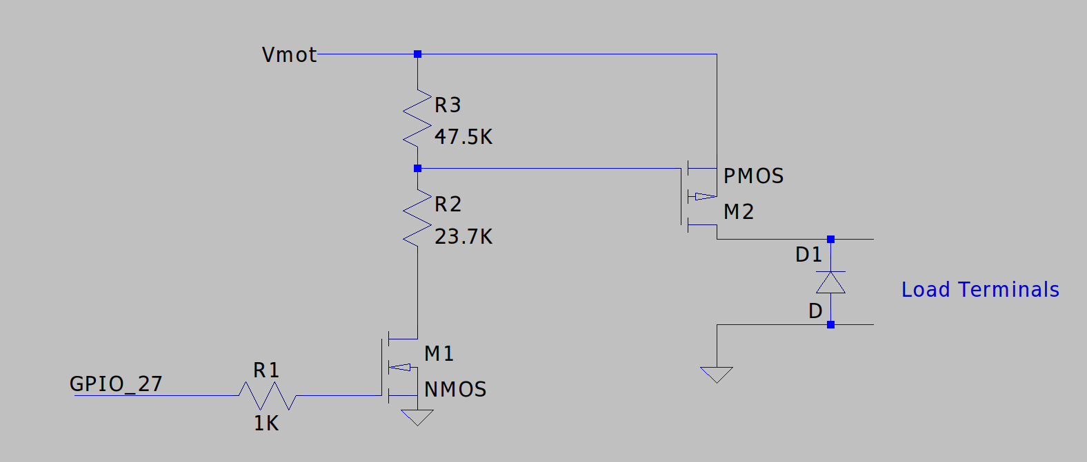
So ignoring the input voltages for now, we’ve got 3 states that GPIO can be in: +3.3V, 0V and open-circuit. Let’s just look at that first FET.
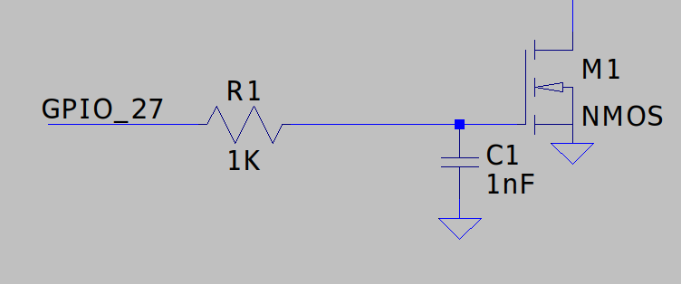
The gate of the FET has a significant amount of capacitance so we definitely want to keep that 1K resistor there. When the GPIO goes from 0V to 3.3V then for a brief period the GPIO pin will be 3.3V while the capacitor is still 0V. 3.3V will be across the resistor so a 1K resistor means a maximum switching current of 3.3mA, which is conservative.
GPIO High-Z/Open-circuit: With the open circuit case we never want to have a FET’s gate open circuit because that’s an undefined condition and something as simple as someone switching on a router nearby could provide enough EMI to make it turn on/off rapidly, etc. So we use a pull-up or pull-down to get it in the state that we want it. This should be mandatory for any GPIO where the micro is configuring it as an output after booting. The output WILL be open-circuit during flashing, incorrect firmware issues, firmware crashes, that kind of thing, so we need to account for it. In this circuit, 0V on the GPIO pin is ‘off’ for the output so we use a pull-down.
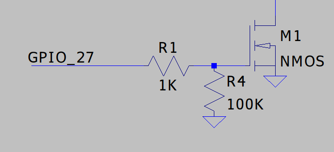
The choice of value for the pull-down is somewhat arbitrary, it needs to be low enough resistance to reliably control the gate to be 0V under all conditions but high enough impedance that you’re not creating a voltage divider with R1 and lowering Vgs unnecessarily.
GPIO at 0V: This is relatively straightforward, both R1 and R4 are connected to 0V so Vgs on M1 will be 0V. For that FET, this is ‘off’. There is usually a drain leakage spec that’s worth being aware of. For the AO3400 that’s 5uA at Vds of 30V. So even when off, it’s worth remembering that there could be 5uA of current flowing through the FET itself. That might be a side effect of the FET being intended to high current loads… That spec is at 30V and it’ll drop as Vds drops so it’s not like it will pull any load that’s connected all the way to 0V, but 5uA is a nice ‘worst case’ spec that means that if we’re ok with 5uA, we don’t need to look at it further. If 5uA is questionable, we know it won’t be 5uA because the voltage would start to drop at that stage, anyway, but it shows we need to figure it out properly…

GPIO at 3.3V: With the added 100K resistor, this is now a voltage divider. 1K over 100K means that the voltage at the gate is 100/101 * 3.3V = 3.27V. Looking at the graphs in the FET datasheet there are a couple that define how the FET works vs applied gate voltage. The ‘proper’ one is Id vs Vds with multiple lines for different Vgs values. In that datasheet it’s Figure 1: On-Region Characteristics, but it can be called all sorts of things.

From this, we look at the 3V line because that’s the closest conservative number. That shows that this FET is way overkill for the job of driving a few high-impedance resistors and could easily be down-sized, which would help with any potential leakage issues, as well.
So that then gives our FET M1 two states, on which is close enough to 0R in our case and off, where we might want to check on the leakage current.
The next stage is the gate drive for the high side P-channel FET. This is basically the same as the N-channel FET on the low side, but the drain/source is ‘flipped’ and the applied gate voltage needs to go more negative to turn on, so we’re looking for what voltage is across R3:

Here the bottom side of R2 can be connected to 0V or open-circuited so we think about those two states. The supply I’ve labeled as Vmot could be as high as +29V or as low as 5V, so we’ll follow those through. The leakage from above is worth thinking about, briefly, just as a sanity check. The total resistance there is ~70K and 5uA through that is 0.35V. Not enough to worry about for this situation, so that’s fine.
Considering the circuit being driven from Vmot = 29V, that gives us 2 options. M1 being on gives us a voltage divider between 29V and 0V. M1 being off is just a straight connection of the gate to 29V.
M1 off:
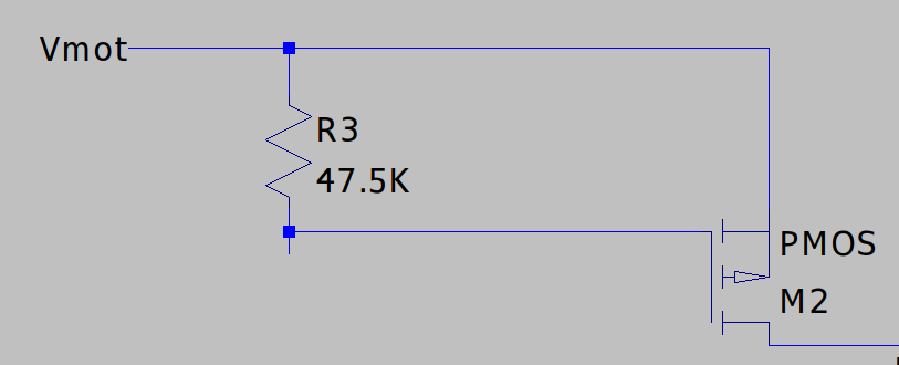
Straight connection of the gate to 29V via R3 is pretty much the same as the 0V condition on the N-channel FET from above. It’s basically just R3 between the gate and source so we can be confident that Vgs will be around 0V and the FET will be ‘off’. We can look and make sure the leakage is ok, but as long as we’re not driving high-impedance loads like logic inputs (cough, cough) then we’re fine. Ids leakage at -28V is specified as 5uA max so we just need to remember that ‘off’, again, could be as much as 5uA. If the input impedance on the device we’re controlling is 1Meg or higher then that ‘could’ potentially be 5V on the output when off, so having something like a 100K resistor across the output terminals might not be a bad idea, just to be sure. This is a slow/DC consideration, though, not a faster switching consideration.
M1 on:
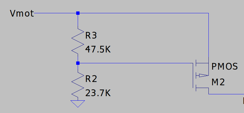
Voltage divider between 29V and 0V, so we need to know what the voltage across R3 is. I don’t know how comfortable you are with doing basic voltage divider calculations like this, but it’s worth thinking about them enough that they become second nature because they come up all the time, as I’m sure you’ve seen. I look at it as the current through the resistors will be R3+R2 and then the voltage we want is across R3, which is the current through R3 * the resistance. Current is V/R, Voltage is IR so that’s current = Vin / (R2+R3), Vout = current * R3, simplified that’s Vout = Vin * R3/(R2+R3). As long as you’re ok using your own logic to figure out the ‘direction/sign’ of the resulting voltage, I always just immediately think of it as a ratio, being the resistor we want the voltage across over the total then multiply that with the input voltage. The voltage we want is over R2 which is 47.5K, the total is R+R3 which is 71.2K so the ratio is 47.5/71.2 because the K suffixes cancel. 0.667 is the ratio. 29V in, 290.667 = 19.3V. We know that we’re working with Vgs so it’s the voltage of the gate vs the source, so that 19.3V is actually a Vgs of -19.3V. Close to the absolute max but not terrible given that we’re already at a reasonable ‘worst case’ input voltage. As long as the resistors are 1% tolerance, the output of the divider will be roughly 1% so maybe -19.5V. That’s ‘fine’.
Considering the circuit being driven from Vsupply = 5V then we only need to consider the M1 on condition because M1 off is the same, just 0V on Vgs.
M1 on: Voltage divider between 5V and 0V, voltage across R3 is the same 0.667 * 5V = so Vgs = -3.34V. That’s low enough that I’d always want to consider the resistor tolerances, but you can approximate that as a 1% change in resistance = a 1% change in divider ration so -3.34 * 0.99 = -3.30V. Worst case Vgs(th) is -2.2V so we know the FET will be ‘on’, technically, but that threshold is defined as where you’ve got 250uA through the FET with no voltage change so it’s not exactly going to drive any big loads!
![]()
Going down to the -Id vs -Vds graph there’s a -3V Vgs curve. That’s close to our situation so we can use that. That will be relative to the ‘nominal’ Vgs(th) number of -1.2V so that’s actually not -3V, it’s more like -1.8V beyond the threshold voltage. Compared to the worst-case Vgs(th) of -2.2V, that would be more like -4V. So we know that line is actually optimistic compared to where we’re at. That means we don’t actually have enough data to be sure what the FET will do under worst case scenarios, which can be a tricky scenario. One option would be to test every board to make sure it works ok at 5V and a specified load. Another would be to talk to the manufacturer about getting the correct data. Another would be find a different FET. Another would be think about how to change that applied gate voltage to be nicer. Another would be ‘yolo’ and hope that the one-in-a-large-number chance of it being an issue doesn’t bite someone too badly.

If we just take the easy road and assume the -3V line is good enough, we can look at that and figure out a Vds/Ids combination that works for us.
Specification of the actual output FET:
Starting with the thermal performance, the junction-to-ambient spec has a note that says it’s on 1in^2 of 2oz copper, which is probably pretty reasonable. That gives 125degC/W as a thermal impedance. Max junction temperature is 150degC so if we say 130degC max to give some headroom and a max operating temperature on the PCB of 50degC then that’s a delta of 80degC. That delta at 125degC/W is 0.64W of dissipation allowed.
Considering the -19V Vgs situation: That’s well beyond all of the specs provided for the FET in the ‘on’ state, so we can use the table data without worrying too much. The device is rated for -4.5A at Tc=100degC so I’d halve that and say that’s probably an easy usage point, so -2A and we don’t need to think much more on it. If we’re above that or want to be sure, we can go to the datasheet we can look at the power loss/thermal info a bit more closely. Looking at the Rds(on) vs -Vgs graph we can doubly confirm that we’re well and truly in the on-state at -19V. From the characteristics table we’re at a worst case of 40mR at 25degC and -10V Vgs. From the normalized Rds(on) vs Tj graph we can see that at 140degC our Rds(on) is maybe 1.7x what it was at 25degC so our actual worst-case Rds(on) is around 40 * 1.7 = 68mR. Power = Current^2 * resistance so current = sqrt(power/resistance). Our output current can be sqrt(0.64W / 0.068R) = ~3A. Also, because we calculated this at 10V Vgs, we know that this should be good for a lot of lower supply voltages. In fact, using the 0.667 ratio of Vsupply to Vgs we calculated above, we can say that it’ll be true until Vmot = 15V. Below that it’ll start to drop so it may be worth figuring out another point, such as minimum input voltage for a 12V system, etc.
Considering the -3V Vgs situation: Same as above but with a bit less confidence in what the datasheet is saying because we’re on the ‘bad’ side of where the information ends. If we just stick to assuming it’ll be fine, that’s Vgs = -3V. We know we’ve got 0.64W to play with and we know that, from the previous calcs, that the Rds(on) will be 1.7x worse at temperature. This is a slightly annoying calculation to do because we don’t know the Rds(on), we have to calculate it from the graph and it relies on the current, which is also what we need to know to calculate the power. One way to do this is just guess-and-check until we get close. The better way would be to pull the Id vs Vds curve out using a plot digitizer and calculate that way. I’ll just do guess-and-check here. So if we say 2A, that appears to be about ~0.17V Vds. A ‘sketchy’ way to check that is to expand the graph on your screen as much as possible and then just use calipers or a ruler ![]() . That really only works well when you’re checking a number that corresponds with a gridline, though, so plot digitizers are better. In my case, I zoomed in until 0.5V was 140mm and the line is at ~46mm so 0.164V. It’s not worth being ‘too’ precise, because the data can be a bit lumpy at that point, but it’s better than nothing.
. That really only works well when you’re checking a number that corresponds with a gridline, though, so plot digitizers are better. In my case, I zoomed in until 0.5V was 140mm and the line is at ~46mm so 0.164V. It’s not worth being ‘too’ precise, because the data can be a bit lumpy at that point, but it’s better than nothing.
0.17V at 2A = 0.085R. We know at temperature it’ll be 1.7x that so 0.145R. 2A at 0.145R = 0.58W. That’s close enough to our loss budget of 0.64W and in the conservative direction so I’d say 2A at 5V is fine. If I were very far away or over the budget I’d adjust and check at say 1.5A. With that graph it’d be difficult to check both so I’d digitize it, put it in a spreadsheet and calculate each point.
Plot digitizer:
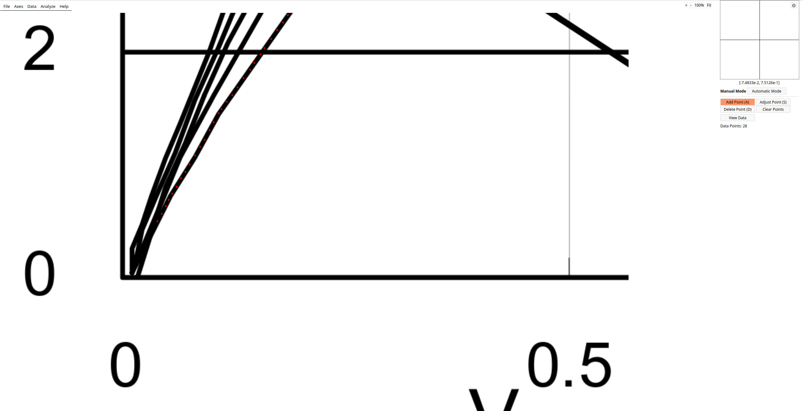
That’s what the lower cell of the -Id vs -Vds graph looks like in WebPlotDigitizer with some points added (the red dots). I ignore the very low points because they’re in a mess on unknown lines and they’re not what we care about anyway. Pasting that data into a spreadsheet lets me add a field for Rds(on) typical which is just Vds/Ids, Rds(on)max which is just Rds(on) typical * 1.7 from above, and then loss which is Ids^2*Rds(on)max.
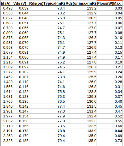
From there we can see our max output current before the FET gets into worrying thermal territory is 2.19A, assuming -3V Vgs and hoping we don’t ever see the absolute worst case FET -Vgs(th).
That whole thing took maybe 2 hours to write out but is really maybe 5 minutes work, max. I would encourage you to keep a spreadsheet attached to every design you do and then create a new sheet in that for each design section. I’d have a sheet for that output stage, for instance, as a place to keep data like the above and a way to make notes about assumptions. It’s then good practice to transfer the important bits into the schematic. I’d make a note saying something like Id(max) = 2A at 5V, 3A at 24V.