In hopes of adding another output pin to the Jackpot2, the config files will be different. So to make future support easier I am bumping the release number. Continued from here, Jackpot V2 - #687 by vicious1
Jackpot3
Specs to follow.
In hopes of adding another output pin to the Jackpot2, the config files will be different. So to make future support easier I am bumping the release number. Continued from here, Jackpot V2 - #687 by vicious1
Specs to follow.
Current issues are
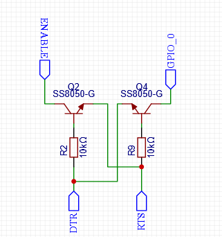
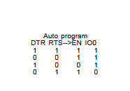
I am not confident I can add anything to gpio.0 and not mess up the USB control. I know the RTS can pull gpio.0 low to enter programming mode but how strong is it pulling? Wrong pull up on my end and that doesn’t work. That also leaves me with a reverse logic pin, the other three will be low triggering high. This is too far over my head, esp32 boot, boot button, USB logic, buffer all on one pin.
Options seem to be;
1- Don’t use it.
2- Leave it floating, use :pd so after boot the pin pulls itself low, the other three output pins will actually be pulled down. Leaves us with one uncertain pin at boot, the other three should be stable.
3- Use the buffer enable. To use the enable feature we would need a timed output so it would not cost us a pin to use, as I am not seeing any other pins that pull low after boot.I still don’t see how to use a pulled up gpio.0 to work with this buffer (is there a reverse logic buffer?), it leaves me with an always on pin that can switch off after boot? What value pull up?
Okay looking at the Corgi, Bart left GPIO.2 floating then pulls it up after boot. Same requirements as GPIO.0 so I will leave that one floating, then pull it down after boot.
Nice, one problem solved.
Looks like the Corgi is also dual voltage. I wish I would have noticed this sooner…
He does not even have a selection jumper or switch both circuits are always active. Feels weird like it could interfere with the signal somehow, but what do I know. Simple, I don’t hate it. Just need to try and make it high side switching 12-24v capable.
Okay, I can’t wrap my head around the high side switching with a p-channel. I think I get it, but not confident enough. A few days of reading in circles is enough. Back to the proven low side switching from the JP1. I feel like I understand it but from what I am seeing I do not understand why the JP2 24V pwm doesn’t work any different. The Vgs is way over the threshold, but the results are the same. So I am still not understanding something.
Seeing the Corgi split output just makes that seem dead simple.
New problem, no room for all the extra terminals.
It MIGHT be possible to get a 4th of the current gray block, but 4 more on top of that can’t happen and still fit a module.
I have been digging through all the different connectors I have around here, on all the random boards I have, modules, LCSC. I do not want to make the board larger.
These sorts of choices are rough.
I need to make the 4 outputs switchable. High side switching of the 24v would mean a common ground and only one wire would have to be switched (5v signal / 24v signal) same ground. The low side switch means both + & - need to be changed.
So back to p-channel or other high side switching. That is the motivation I needed not to do it the easy way.
21 posts were split to a new topic: IOS discord forum issues
I didn’t think we could have two live circuits like that. Seems like odd things could happen. I am getting closer to the high side stuff. Just need the reason to spend more time on it.
You mean a single gpio driving multiple different circuit elements?
No problem as long as you understand the requirements of each leg and she underlying interface requirements for each side and for a generic pin like a GPIO you have to think of all the ways a user might configure it.
I don’t think that’s a problem as long as it fits instead the beam. ![]()
I keep asking this out of context - why does it have to be in the beam? Is it valid to question why we don’t move all of the bits back to a box on/under the table?
I’m on board with you here (pun intended)
If it fits inside the beam it can also fit in a box though, whereas the opposite is not guaranteed
So maybe it’s a good thing to take this as a constraint and let the user choose?
Under the table means the X, Y2 and Z2 would need to be about 10’ wire minimum. And all those wires would need to be managed very well to keep things moving well. At that point the removable part of the machine gets invalidated, and to me that is a key feature in a small shop.
Agree. It can always be moved under the table if one prefers.
So this became a non point when our systems were ran without lcd. We now have wireless communication and that means shorter wires like Ryan pointed out. It is all preference.
I suggested that a few times above ![]()
If there’s nothing on the output, it doesn’t matter. It’s very common to have digital outputs that aren’t connected to anything and are switching away merrily. It’s how we do test points etc. It’s also no issue for the open-drain outputs because they probably don’t end up even doing anything under switching conditions because there’s nothing other than a tiny bit of leakage current through the flyback diodes to pull them high, so they’ll just look like they’re always at 0V until someone adds a load.
I will note that they use low-side switching on that board, but the same principle applies to the high side circuit from above.
What specifically are you struggling with here? It’s pretty simple, I would encourage you to just break it down into a simpler set of ‘goals’ for each part and then calculate those for each state.
What specific issue are you referring to here? What works and what doesn’t? Threshold voltage isn’t everything, it’s just a point where the switch ‘starts’ to turn on. It’s not like a relay or solenoid valve, it’s more like a servo connected to a tap. There’s a minimum amount of gate voltage you need for it to reach an arbitrary amount of ‘on’ (say the tap starts to drip, for instance), and then you need to add more beyond that to get it to be on enough for whatever your goal is. A little bit more might be fine if you’re ok with a trickle of water (equivalent to a low current load like a small fan), because the load will have most of the voltage drop across it. If you want to really flow a lot of water (equivalent to a high current LED strip or maybe even a DC motor used as a spindle) then you need to give it a lot more gate voltage. This data is in the datasheet as a Vds vs Ids curve which will show you how much ‘voltage drop’ there is over the FET vs current and should have ~5-10 different curves for different gate voltages. That issue is why it’s very hard for find good power FETs that’ll handle 3.3V supply, for instance.
Could use the same terminals and select which circuit drives them with jumpers. Care needed to avoid killing stuff downstream, of course, but that seems a fair trade.
Just checking that people are discussing the right things… Seems like there are several options here: Inside the beam, inside a box attached to the beam, off the beam entirely (on one of the trucks, perhaps?), mounted to the table somewhere.
I can see the logic behind avoiding the off-beam options due to wire routing lengths starting to increase etc. but realistically how important is ‘in-beam’ vs ‘on-beam’? Personally I don’t see an issue and would rather easier wiring and better functionality in that circumstance.
So that’s what we’re starting with. Let’s go through a steady-state analysis. This is assuming that everything doesn’t mind being turned on or off slowly and is focused on the DC state that things get to eventually. It’s a good starting point.
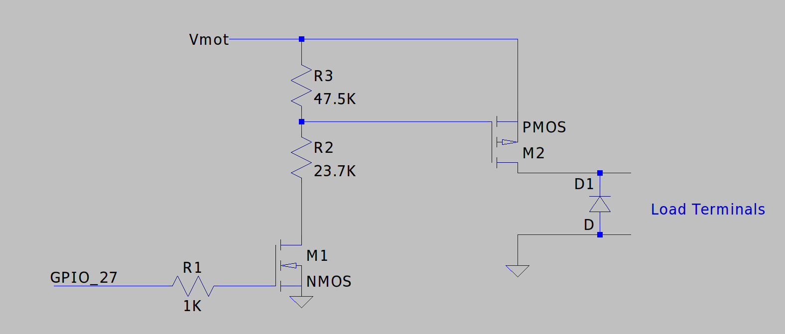
We’ve got 3 logic input states to deal with, logic high, logic low and high impedance. We’ve got 2 desired output states, ‘on’ and ‘off’. We’ve got 2 different supply voltages, +5V and Vmot. Vmot has a range that it can realistically be so usually we’d define a highest and lowest but in this case 5V is below the lowest Vmot so we just need to think of highest, which is 24V + 20% or so, so roughly 29V, or whatever the input over-voltage protection is set at, etc.
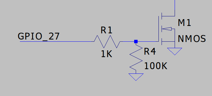
So ignoring the input voltages for now, we’ve got 3 states that GPIO can be in: +3.3V, 0V and open-circuit. Let’s just look at that first FET.
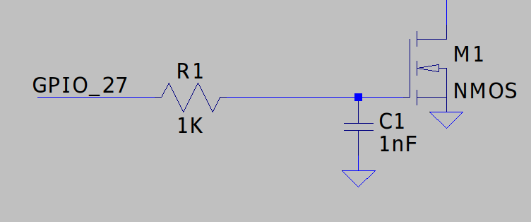
The gate of the FET has a significant amount of capacitance so we definitely want to keep that 1K resistor there. When the GPIO goes from 0V to 3.3V then for a brief period the GPIO pin will be 3.3V while the capacitor is still 0V. 3.3V will be across the resistor so a 1K resistor means a maximum switching current of 3.3mA, which is conservative.
GPIO High-Z/Open-circuit: With the open circuit case we never want to have a FET’s gate open circuit because that’s an undefined condition and something as simple as someone switching on a router nearby could provide enough EMI to make it turn on/off rapidly, etc. So we use a pull-up or pull-down to get it in the state that we want it. This should be mandatory for any GPIO where the micro is configuring it as an output after booting. The output WILL be open-circuit during flashing, incorrect firmware issues, firmware crashes, that kind of thing, so we need to account for it. In this circuit, 0V on the GPIO pin is ‘off’ for the output so we use a pull-down.
The choice of value for the pull-down is somewhat arbitrary, it needs to be low enough resistance to reliably control the gate to be 0V under all conditions but high enough impedance that you’re not creating a voltage divider with R1 and lowering Vgs unnecessarily.
GPIO at 0V: This is relatively straightforward, both R1 and R4 are connected to 0V so Vgs on M1 will be 0V. For that FET, this is ‘off’. There is usually a drain leakage spec that’s worth being aware of. For the AO3400 that’s 5uA at Vds of 30V. So even when off, it’s worth remembering that there could be 5uA of current flowing through the FET itself. That might be a side effect of the FET being intended to high current loads… That spec is at 30V and it’ll drop as Vds drops so it’s not like it will pull any load that’s connected all the way to 0V, but 5uA is a nice ‘worst case’ spec that means that if we’re ok with 5uA, we don’t need to look at it further. If 5uA is questionable, we know it won’t be 5uA because the voltage would start to drop at that stage, anyway, but it shows we need to figure it out properly…

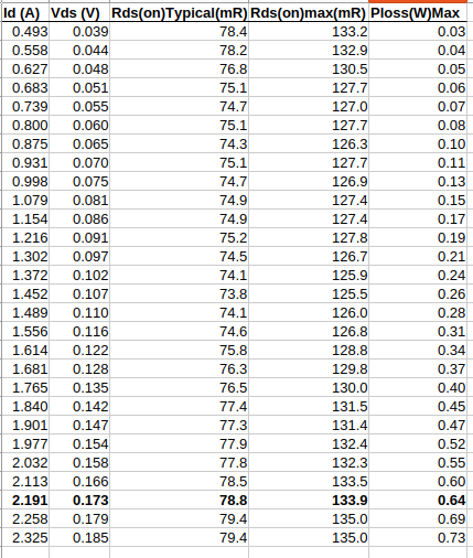
GPIO at 3.3V: With the added 100K resistor, this is now a voltage divider. 1K over 100K means that the voltage at the gate is 100/101 * 3.3V = 3.27V. Looking at the graphs in the FET datasheet there are a couple that define how the FET works vs applied gate voltage. The ‘proper’ one is Id vs Vds with multiple lines for different Vgs values. In that datasheet it’s Figure 1: On-Region Characteristics, but it can be called all sorts of things.
So that then gives our FET M1 two states, on which is close enough to 0R in our case and off, where we might want to check on the leakage current.
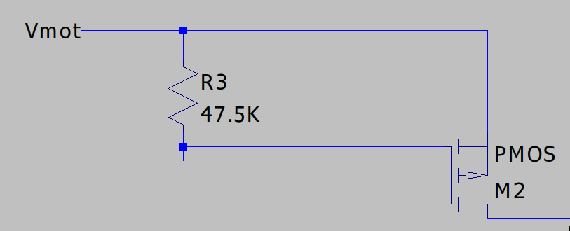
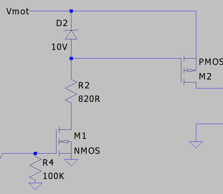
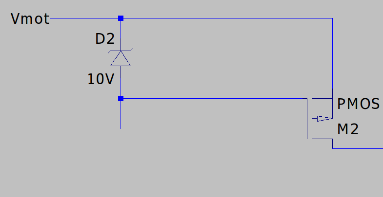
The next stage is the gate drive for the high side P-channel FET. This is basically the same as the N-channel FET on the low side, but the drain/source is ‘flipped’ and the applied gate voltage needs to go more negative to turn on, so we’re looking for what voltage is across R3:
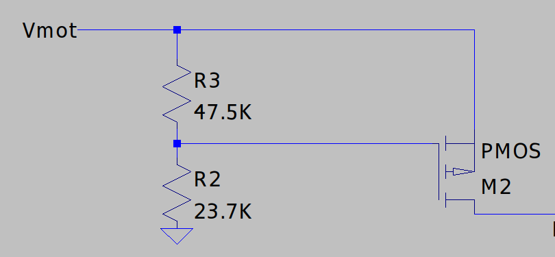
Here the bottom side of R2 can be connected to 0V or open-circuited so we think about those two states. The supply I’ve labeled as Vmot could be as high as +29V or as low as 5V, so we’ll follow those through. The leakage from above is worth thinking about, briefly, just as a sanity check. The total resistance there is ~70K and 5uA through that is 0.35V. Not enough to worry about for this situation, so that’s fine.
Considering the circuit being driven from Vmot = 29V, that gives us 2 options. M1 being on gives us a voltage divider between 29V and 0V. M1 being off is just a straight connection of the gate to 29V.
M1 off:
M1 on:
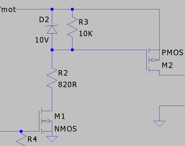
Considering the circuit being driven from Vsupply = 5V then we only need to consider the M1 on condition because M1 off is the same, just 0V on Vgs.
M1 on: Voltage divider between 5V and 0V, voltage across R3 is the same 0.667 * 5V = so Vgs = -3.34V. That’s low enough that I’d always want to consider the resistor tolerances, but you can approximate that as a 1% change in resistance = a 1% change in divider ration so -3.34 * 0.99 = -3.30V. Worst case Vgs(th) is -2.2V so we know the FET will be ‘on’, technically, but that threshold is defined as where you’ve got 250uA through the FET with no voltage change so it’s not exactly going to drive any big loads!
![]()
Going down to the -Id vs -Vds graph there’s a -3V Vgs curve. That’s close to our situation so we can use that. That will be relative to the ‘nominal’ Vgs(th) number of -1.2V so that’s actually not -3V, it’s more like -1.8V beyond the threshold voltage. Compared to the worst-case Vgs(th) of -2.2V, that would be more like -4V. So we know that line is actually optimistic compared to where we’re at. That means we don’t actually have enough data to be sure what the FET will do under worst case scenarios, which can be a tricky scenario. One option would be to test every board to make sure it works ok at 5V and a specified load. Another would be to talk to the manufacturer about getting the correct data. Another would be find a different FET. Another would be think about how to change that applied gate voltage to be nicer. Another would be ‘yolo’ and hope that the one-in-a-large-number chance of it being an issue doesn’t bite someone too badly.
Specification of the actual output FET:
Starting with the thermal performance, the junction-to-ambient spec has a note that says it’s on 1in^2 of 2oz copper, which is probably pretty reasonable. That gives 125degC/W as a thermal impedance. Max junction temperature is 150degC so if we say 130degC max to give some headroom and a max operating temperature on the PCB of 50degC then that’s a delta of 80degC. That delta at 125degC/W is 0.64W of dissipation allowed.
Considering the -19V Vgs situation: That’s well beyond all of the specs provided for the FET in the ‘on’ state, so we can use the table data without worrying too much. The device is rated for -4.5A at Tc=100degC so I’d halve that and say that’s probably an easy usage point, so -2A and we don’t need to think much more on it. If we’re above that or want to be sure, we can go to the datasheet we can look at the power loss/thermal info a bit more closely. Looking at the Rds(on) vs -Vgs graph we can doubly confirm that we’re well and truly in the on-state at -19V. From the characteristics table we’re at a worst case of 40mR at 25degC and -10V Vgs. From the normalized Rds(on) vs Tj graph we can see that at 140degC our Rds(on) is maybe 1.7x what it was at 25degC so our actual worst-case Rds(on) is around 40 * 1.7 = 68mR. Power = Current^2 * resistance so current = sqrt(power/resistance). Our output current can be sqrt(0.64W / 0.068R) = ~3A. Also, because we calculated this at 10V Vgs, we know that this should be good for a lot of lower supply voltages. In fact, using the 0.667 ratio of Vsupply to Vgs we calculated above, we can say that it’ll be true until Vmot = 15V. Below that it’ll start to drop so it may be worth figuring out another point, such as minimum input voltage for a 12V system, etc.
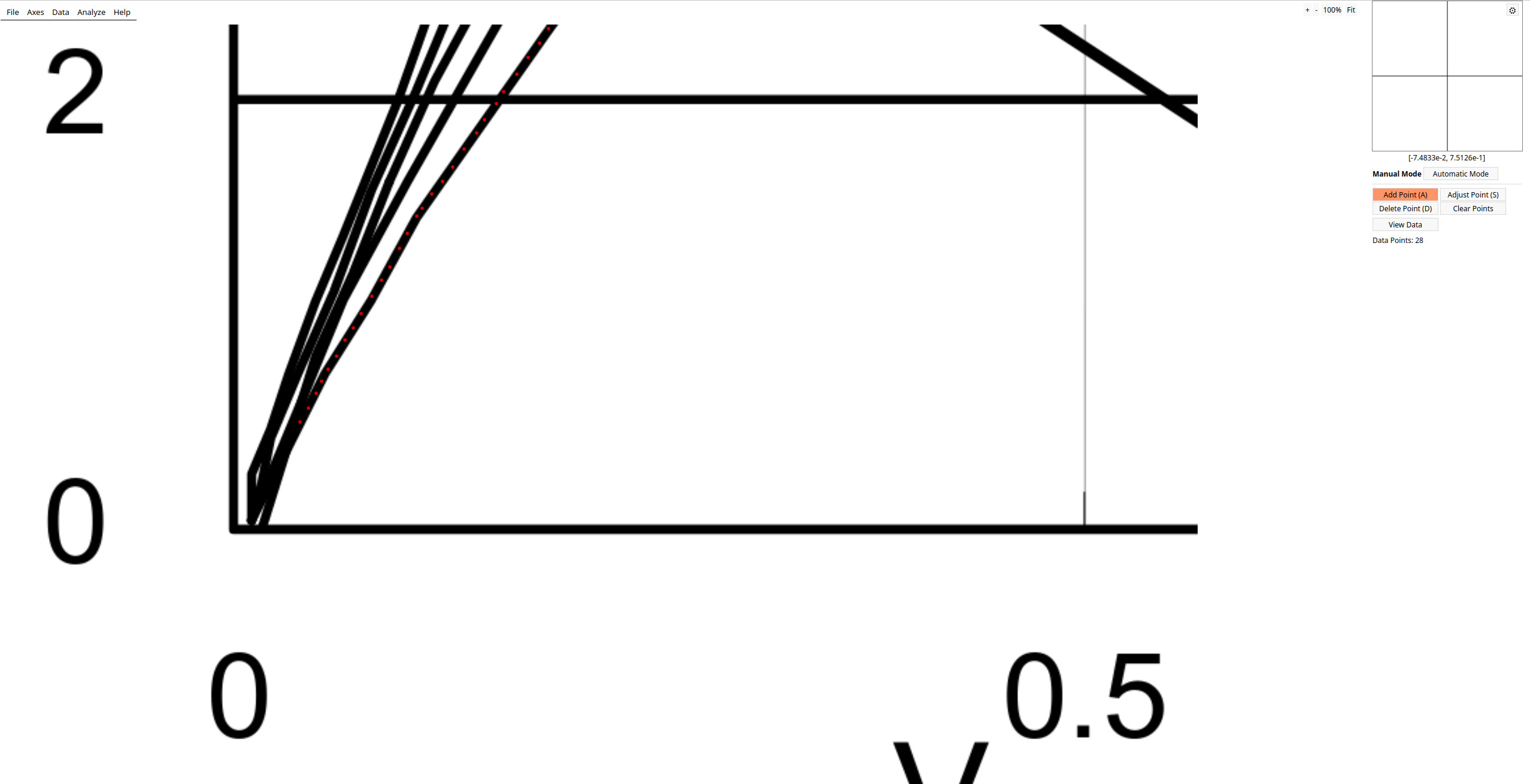
Considering the -3V Vgs situation: Same as above but with a bit less confidence in what the datasheet is saying because we’re on the ‘bad’ side of where the information ends. If we just stick to assuming it’ll be fine, that’s Vgs = -3V. We know we’ve got 0.64W to play with and we know that, from the previous calcs, that the Rds(on) will be 1.7x worse at temperature. This is a slightly annoying calculation to do because we don’t know the Rds(on), we have to calculate it from the graph and it relies on the current, which is also what we need to know to calculate the power. One way to do this is just guess-and-check until we get close. The better way would be to pull the Id vs Vds curve out using a plot digitizer and calculate that way. I’ll just do guess-and-check here. So if we say 2A, that appears to be about ~0.17V Vds. A ‘sketchy’ way to check that is to expand the graph on your screen as much as possible and then just use calipers or a ruler ![]() . That really only works well when you’re checking a number that corresponds with a gridline, though, so plot digitizers are better. In my case, I zoomed in until 0.5V was 140mm and the line is at ~46mm so 0.164V. It’s not worth being ‘too’ precise, because the data can be a bit lumpy at that point, but it’s better than nothing.
. That really only works well when you’re checking a number that corresponds with a gridline, though, so plot digitizers are better. In my case, I zoomed in until 0.5V was 140mm and the line is at ~46mm so 0.164V. It’s not worth being ‘too’ precise, because the data can be a bit lumpy at that point, but it’s better than nothing.
0.17V at 2A = 0.085R. We know at temperature it’ll be 1.7x that so 0.145R. 2A at 0.145R = 0.58W. That’s close enough to our loss budget of 0.64W and in the conservative direction so I’d say 2A at 5V is fine. If I were very far away or over the budget I’d adjust and check at say 1.5A. With that graph it’d be difficult to check both so I’d digitize it, put it in a spreadsheet and calculate each point.
Plot digitizer:
That whole thing took maybe 2 hours to write out but is really maybe 5 minutes work, max. I would encourage you to keep a spreadsheet attached to every design you do and then create a new sheet in that for each design section. I’d have a sheet for that output stage, for instance, as a place to keep data like the above and a way to make notes about assumptions. It’s then good practice to transfer the important bits into the schematic. I’d make a note saying something like Id(max) = 2A at 5V, 3A at 24V.
Soooooooooo…
Assuming that’s all good then fine, run with it.
If you’re worried about the gate voltage being too low at 5V and too high at high Vmot, there are a couple of options mentioned above.
One would be different FET, maybe one that has a lower Vgs(th) or a higher Vgs(max). That gets really annoying to try find and honestly I’d probably not bother, the one there looks pretty middle-of-the-road.
Another would be trying to figure out a way to change the voltages applied to the gate. The easiest way to do that would probably be to put a zener diode in to clamp the voltage. Another way would be to change the resistors as needed using a jumper etc. You could also use some tricksiness and use PWM on GPIO_27 to apply say a 50% duty cycle to M1 when you know that it’s set to 24V input mode, but then you’ve got issues with breaking stuff if it goes wrong etc. etc.
The zener approach:
For circuits like this, I like to design them in the most ‘extreme’ form first and see if that works. Let’s say we want as close to 10V on the gate at all points, we could just add a 10V zener to clamp it if it goes above that.
If we want R2 to be a standard 1/8W resistor, we should be aiming for half that ideally, so 1/16W or 62mW. P=V^2/R so R = V^2/P. 20V^2 / 0.062 = 6.5K. Nearest E24 would be 6.8K so 20V/6.8K = 2.9mA. 2.9mA in a 6.8K resistor is 57mW. 2.9mA through the 10V zener and 10K resistor is 29mW, which is clearly fine for both of those. At 5V that will be a 10K over 6.8K voltage divider 5*10/16.8 = 2.97V and we’re back where we started.
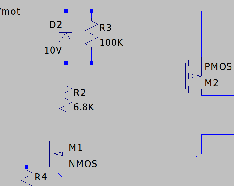
To solve that we raise the impedance of R3. Let’s say to 100K to match R4. Now that’s 100K over 6.8K so 5*100/106.8 = 4.68V. 5uA of leakage through M1 is 0.5V worst case.
That circuit gives us -10V Vgs for the 24V input case and -4.7V Vgs for the 5V case. It has a little more loss when the output is on (~100mW) but nothing too major. I would double-check that the zener is specified for operation at 3mA, some of them specify 5mA or 10mA depending on voltage. That just means that the voltage might not be super accurate, which may not bother us as long as the FET performance is good enough.
We could also push that further by using say a 15V FET and lowering the impedance of R2 etc. but that all gets into the type of thing that’s easier to do with a spreadsheet so you can look at 4-5 different options in parallel.
Different resistor approach:
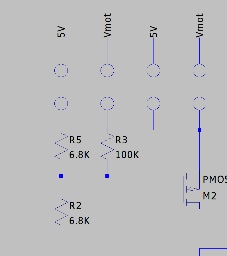
You could also have it such that the resistors get modified along with the input voltage:
Duplicated circuit approach:
You could have a 5V and Vmot circuit each with their own P-channel high-side FET and then the jumper just selects which one you want. Bit ugly due to duplicating parts but maybe a couple extra $ is worth it?
High side switch IC:
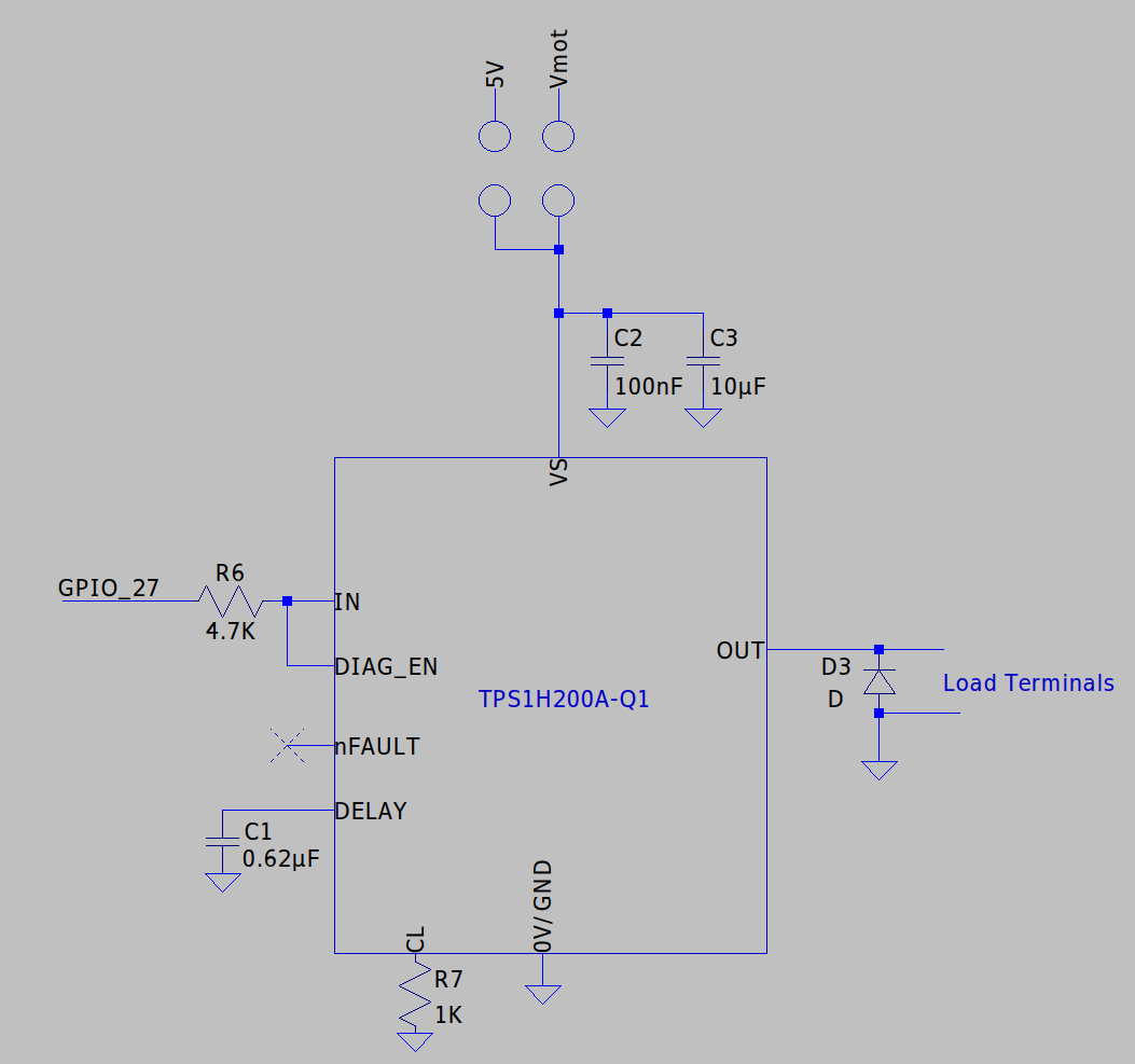
There are integrated high-side switch devices you can buy like this:
That’s just an example but it’s a 8pin SSOP package a thermal pad. It’s rated at 2A and has adjustable current limit with feedback etc. Operates from 4V to 40V. 3.3V logic compatible inputs (1.8Vmin for VIH).
That’s how I’d implement that. There are a couple of notes there about protecting against reverse polarity but I don’t think they’re that relevant. For protecting against input power failure an external free-wheeling diode is recommended. A 4.7K resistor in series with the IO is recommended by the datasheet.
It’s worth noting that these high side switches are still intended for loads, not logic output so they’ll be too slow to use for PWM.
The better solution, still, for PWM is to either use different FETs or a digital buffer on a different connector, even if that’s not an ‘ideal’ option such as a pin header etc. Or have the load always at 24V, the logic always at 5V and then jumper select between the 2 circuits.