Right. My apologies, I had forgotten that you might still be trying to speed up the high-side switch state. A week of being out of town for work kinda factory reset me a little. That makes my 2 hour rant a little less relevant.
Unfortunately timing stuff gets complicated quickly. Not impossible, just harder. The kinda ‘short story’ there is that if you want things to be fast, it’s better to have driven logic where both the rising and falling edges are caused by FETs switching, not just driven in one direction and then allowed to be pulled/float down in the other direction. It’s not impossible for the latter to be fast, indeed that’s how I2C works, but it’s a lot more difficult and requires significant design time to verify it all.
Given that we’re already switching between 5V and Vmot, is there any specific situation where we would absolutely need PWM at Vmot or 2A drive at 5V? Powering something significant from 5V should probably be done by an external step-down converter at 24V anyway. Most things that can accept a PWM signal should be fine at 5V?
Yeah, kinda. Basically the FET is a voltage controlled resistor. As you apply voltage to the gate it creates an electric field across a piece of semiconductor that creates a conductive path, essentially squeezing it shut or opening it up, depending on the type of FET. Again to use the water analogy it’s like a ball valve that’s servo controlled. No voltage applied, no opening. A little bit of voltage applied, say 2V, you get the first drips. Beyond that, the valve just opens more. Even at 8V or 10V, the valve isn’t fully open, but it’s open enough that going from 2V to 4V makes a huge difference, 4V to 6V less so, etc.
All of this isn’t really anything to do with ‘speed’, as such. If all you’re trying to do is catch a drip and we don’t care what happens afterwards, giving it 2V will be as fast as 10V. That’s basically capacitance. Trying to fill a thimble would be small capacitance, trying to fill a barrel would be a big electrolytic capacitor. The issue is that big FETs (big valves) have big output capacitances (I guess the analogy would be large pipes) to ‘fill’. The other aspect is that the gate itself is a capacitor that needs to be filled, so you’re controlling your ball valve by filling up a bucket of water. Big, high current FETs have big buckets to fill to control how much they’re on. Small, low current FETs have small buckets and can be filled quickly.
As an interesting aside, when we’re dealing with switch-mode power supplies, we want that FET to switch as fast as possible usually, because while it’s half on you have high current and high voltage across the FET, which means lots of loss. You can never switch instantly, but we try to minimize it. ‘Fast’ at 1200V/100A would be in the 20-40ns range. That’s switching a very big FET with very large capacitances very quickly. To do that, we need to put a lot of current into the gate. We do that with dedicated ICs that do nothing but take the logic input and turn it into a very high current output specifically designed to quickly fill/empty those capacitors. Our ‘standard’ sized gate drive was about 9A peak output current at +18V/-5V, so basically +24V of voltage change at 9A peaks. Overall only around 1-2W per FET, but we would have 8-10W of circuitry that’s there just turning the FETs on and off. That’s pretty close to the same power used to drive the motion stage in an LR4!
It creeps up on you quickly. 10kHz is pretty slow, 100us periods isn’t too bad. Then once you add PWM to that, it quickly becomes that you don’t really want 10kHz, you want 10kHz at say 14% duty cycle. Which means you’re now talking about a 14us pulse every 100us. If you want that 14us pulse to be accurate, you really need your rise and fall times to be ~10% of the minimum width to have it still look like a square wave and not have a huge offset. That’s suddenly 1.4us rise and fall times. Still pretty slow relative to most logic, but enough to be irritating in this scenario.
100% understood, and I think this is where doing this ad-hoc and via forum posts is making it a little difficult. These are all basic techniques that would be quick to cover in a learning environment or as explaining things, but the friction behind asking questions about that and writing the answers out is enough to slow it down.
Basically, though, pretty much everything should have some form of series resistance to limit peak currents and everything should have some form of pull-up/pull-down to control states during high-Z periods.
Dealing with plumbing analogies definitely gets limiting, but not impossibly so. You’ve just gotta keep in mind that they’re a limited and imperfect means to understand one single concept at a time, not a cohesive set of rules that maps perfectly. A FET is a ball valve with a bucket hanging off the handle and a spring pulling it closed. Fill the bucket with water (charge the gate capacitance), the valve opens more (the conductive channel forms/widens). Empty the bucket (discharge the gate capacitance) and the valve closes more (the channel shrinks/pinches). The more open the valve (the more open the channel, the lower the channel resistance), the more water flow/less pressure drop (less voltage drop for a given current, more current at the same input voltage) etc. Trying to map anything onto that further gets difficult. The valve has no inertia and no resistance to being turned. The valve overheats if it’s partially open and there’s lots of flow through it. That heating is the main way we choose valves and you can have 2 valves that have the same size orifice when fully open but that can handle different flow rates for different periods of time. All of that you can kinda hand-wave your way into, but it just gets less and less useful compared to just explaining the underlying physics. The thing controlling the flow of electrons isn’t physical, it’s an electric field and charge carriers in a semiconductor. The specifications of the FET isn’t solely defined by the silicon die itself, but also the package it’s in, the leads that are connected to it and the cooling solution used. Different methods of physically making the FET in terms of how it’s layered up in 2D/3D space and how things are connected together internally can mean that 2 devices with the same voltage/current/resistance in the datasheet may perform very differently in terms of speed, how they switch, what it takes to drive them, etc.
Go for it. It doesn’t have to be a ton of time, but the 2nd best time to start is now. Even doing a little bit at a time is good because it can shake questions loose that we can answer here or that may clarify something you’ve already learned in a way that connects it back to something else etc.
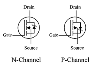
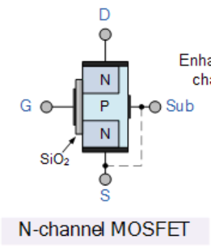
Yeah, P-channel FETs are kinda awful like that. They’re actually somewhat uncommon to use these days as discrete parts, they’re in almost every piece of silicon ever but normally in an integrated circuit so you’re not dealing with them directly. If you look carefully at the symbol, you’ll see they’re often drawn into a circuit upside down because that’s what allows us to stick with the convention that current flows from top to bottom and left to right. No reason for that other than convention, of course, and in reality positive current is negatively charged electrons flowing backwards etc. but it’s best not to stare into that particular void for too long!
So that’s a ‘right way up’ drawing of an N-channel and P-channel enhancement mode MOSFET. If they show the body diode then that’s the easy way to identify them in that it’s backwards compared to the other type, but the actual definitive thing is the arrow. You may not be aware of this, but the diagram of the FET actually represents the way the semiconductor itself is physically constructed, at least in a somewhat abstract way. There is a ‘strip’ of semiconductor that gets ‘doped’ (essentially that just means forcing impurities into the pure silicon so it has either excess electrons or excess spaces for electrons to be) such that it almost conducts but doesn’t quite have enough charge carriers. On either side of that strip are insulated conductors that forms the plates of a capacitor with the strip in the middle. As the capacitor is charged up, an electric field is created that causes charge carriers to get pulled into the strip such that it starts to become conductive. More voltage on the capacitor plates means stronger electric field which means more charge carriers come in which means lower resistance.
The G and Sub connections are to 2 black lines that represent the plates of the capacitor. Sub just means ‘substrate’, because that’s how it’s made, usually that’s just the bottom of the stack and where things get stuck down via. The D and S connections are at either end of the semiconductive strip. Looking at the symbol for the MOSFET again, you can see how the lines match up to their respective physical counterparts. The big unbroken line connected to the gate represents one side of the capacitor. The 3 shorter lines opposite it are the 3 other connections to the semiconductor. The arrow on the other side of the gate isn’t a diode, it’s telling you how the semiconductor was made and therefore what polarity of voltage needs to be applied to make it change resistance.
The N and P sections denote different types of semiconductor doping, N meaning it has extra electrons floating around unneeded, P meaning it has a lot of missing spots where electrons should be. If it were just a N or P section, it would conduct because electrons flowing in could make it through to the other side. If it were just an N and a P, that’s a diode where it will conduct from P to N (electrons fill the holes in the P section and push through until they knock out the extras in the N section) but won’t from N to P (electrons get bunched on the N section with nowhere to go, more complicated than that but that’s the gist). With the NPN section you’ve got a conventional bipolar transistor that you’d shove electrons in/out the middle of to ‘fill in’ the middle section such that it conducts by connecting the middle P section to the base. Or, you get a FET by making the insulated capacitor plates on either side and using electric fields to ‘drag’ electrons around within the structure, causing the extra electrons from the N endcaps to be ‘sucked’ deeper and deeper into the P middle section, eventually causing a thin strip of uniform N section where current can flow. More electric field, more ‘electron suckage’, wider strip of conductive material, lower resistance. That uniform section that is formed when electric field is applied and where current subsequently flows is called the ‘channel’. N-channel FET means it’s doped NPN and shrinking the P section gets you an ‘N channel’ to conduct current through. P-channel FET means it’s doped PNP and shrinking the N section gets you a ‘P channel’ to conduct current through.
This is all for enhancement mode MOSFETs, which is the most common type. These are devices where the channel is ‘blocked’ to start with and needs to be ‘enhanced’ in order to start conducting. Applying gate voltage creates the electric field that enhances the channel so it conducts. The alternative is a depletion mode MOSFET which behaves opposite. The channel initially conducts so it needs to be ‘depleted’ to turn off, which is done by applying a gate voltage which creates a magnetic field, etc. etc. There are both N-channel and P-channel version of both enhancement and depletion mode MOSFETs, so it gets real confusing. 90% of the time you’ll use an N-channel enhancement mode MOSFET. 9% of the time you’ll use a P-channel enhancement mode MOSFET. The remaining 1% of the time you’ll use a depletion mode MOSFET and, if you’re anything like me, wonder why the hell you bothered because it’s annoying to get your head around! Enhancement mode MOSFETs are so common these days that you don’t even usually need to specify enhancement mode, it’s by far the de-facto standard form. There are also junction FETs which are actually a lot more like the idealised ‘semiconducting strip with plates either side’ I described above but are even less common again in discrete forms. They’re super common in ICs and I guarantee there are millions of them within a meter of you right now, but the roles they are best for aren’t all that common to hand-design out of individual parts anymore. Mostly ultra-sensitive inputs for amplifier stages, more or less.
The FET name is for Field Effect Transistor, basically describing that relationship. Transistor because it’s a shortening from transresistance, basically a changing resistance device. Field effect because it’s controlled by the electric field created between those capacitor plates, rather than by injecting current directly like a bipolar transistor. So pretty much a capacitor voltage controlling a variable resistance. MOS is metal oxide semiconductor, named for the metal oxide insulator that is used to insulate the gate to create the capacitor such that it can be kept separate from the ‘power’ connections.
That’s quite the diversion I just went on, it’s not really ‘that’ relevant, it’s just interesting!
So with the P-channel, it all works kinda backwards, if you look at the symbols with the drain at the top and source at the bottom, current flows from source to drain in the P-channel instead of drain to source like in the N-channel, the applied voltage needs to be negative vs the source in the P-channel instead of positive vs the source like the N-channel. Because of the previously mentioned convention behind current flowing top to bottom we usually draw the FETs upside down. The voltage we care about for the gate is the Gate-Source voltage but now the source is at the top of the device, so it’s the voltage at the gate minus the voltage at the top. As you said before, if the gate is pulled down to 5V and the source is connected to 24V, you’ve got 5V-24V = -19V as your Vgs. For that same reason you’ll see all the graphs in the datasheets are using positive numbers but referencing -Id, -Vds, -Vgs etc. That’s just a convention, again, so that they’re easier to read because they look the same as N-channel devices, just with all the nomenclature reversed.
I mentioned this above but I’ll reiterate it here to directly answer this. There are a couple of different aspects.
The first is that the applied voltage to the gate isn’t really about it switching fast or slow, as such. As above, the drain-source resistance pretty much instantly follows the applied gate voltage. Higher voltage doesn’t mean turning on ‘faster’ or anything, really, it just means turning on to lower resistance. That’s a little bit nit-picky, so sorry about that, but it’s an important distinction later. The next part of it is what you’re doing with that resistance. We’re talking a lot about ‘on’ and ‘off’, but in reality all the FET is doing is being a variable resistor. In this case we’re talking about the voltage at the terminals being high or low, meaning that some other logic device downstream can look at it and say ‘this is logic high’ or ‘this is logic low’.
If we have a lot of capacitance then we need a lot of current to flow through the FET before the voltage starts to change. For that we need to have the FET in a lower resistance state to allow more current to flow and therefore make that voltage change happen faster. If we have less capacitance then we can still have it change voltage fast but without needing to turn the FET on as much, or have it change voltage faster with the FET turned on the same amount, etc.
The second part is that this analysis is what we call a ‘steady state’ analysis. It assumes that everything has settled. I guess the water analogy would be we’re assuming everything is flowing nicely and we’re ignoring situations like taps turning on/off quickly and causing water hammer, things like that.
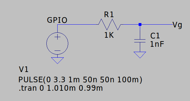
The gate is a capacitor and the resistance of the FET changes based on how much it’s charged. For argument lets say we’re driving the FET’s gate directly via a resistor, like with the low-side FET that’s connected directly to the microcontroller. If we look at this in steady state, 3.3V out from the micro means 3.3V on the gate because there’s nowhere else for any current to go. Let’s say the FET is an imaginary perfect impossible device and its gate has no capacitance. That would mean that regardless of the resistor we use, the gate would look like an open circuit so the voltage on the GPIO pin would be the same as the voltage on the gate. If we instantly change the GPIO pin from 0V to 3.3V, the gate voltage will do the same. In reality that change isn’t instant, but it’s way faster than the issues we’re having so we can call it instant, for now.
In reality, there’s a bit of capacitance on the gate, lets say it’s a 1nF capacitor. Now we’ve got an RC filter that’s created by the resistor between the GPIO pin and the gate. If we assume that the resistor is a 1K resistor then we can use other tools to see what the actual voltage change is at the capacitor (the gate voltage) when a sudden 0V to 3.3V ‘step’ is applied. The best tools for this are things like SPICE simulations which can show things in great detail, but an RC filter is simple enough that they can be fully analyzed mathematically and there are websites that will show you key features.
The short answer, though, is that it takes time for the voltage to change because the capacitor needs current to flow into it to ‘charge up’, and the resistor limits how much current can flow.
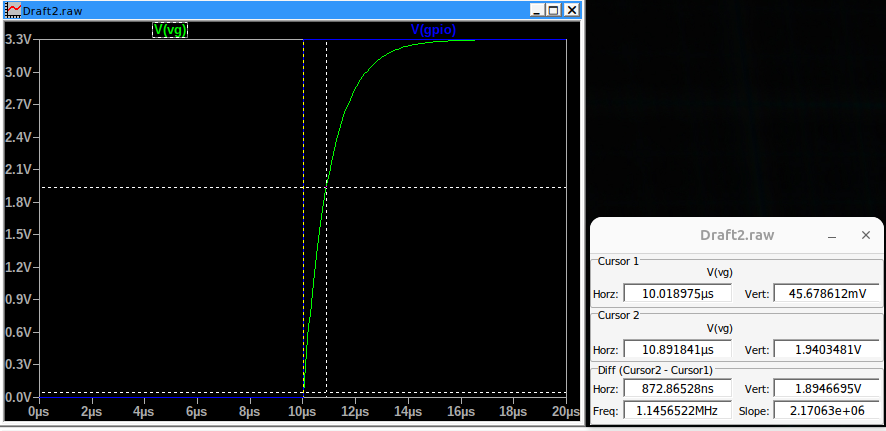
Throwing that circuit into LTspice (the most common freely available circuit simulation tool), I create a voltage source that changes from 0V to 3.3V in 50ns which should mimic the GPIO on the ESP32. That then feeds into a 1K resistor and a 1nF capacitor. I can ‘probe’ the voltages at both the GPIO pin and the capacitor and see what happens as a result.
The blue line is the GPIO voltage, the green is the capacitor voltage and I’ve added 2 cursors which calculates a couple of things. But more or less what you can see with the green line is the characteristic shape that always happens with an RC filter and a stepped voltage response. The neat thing is that it doesn’t matter if it’s 0V to 3.3V, 0V to 100V, 10V to 20V etc., it always looks the exact same and is the exact same time, just scaled to the amount of voltage step that’s applied. That’s because more volts means more current through the resistor but also more current is needed for the capacitor to change to that higher voltage. It’s always linear.
So from this we can see that if we’re looking to go from 0V to say 1.9V, the step happens at 10us into the simulation and the green line (gate capacitor voltage) passes 1.9V roughly 900ns later.
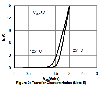
As we’ve discussed before, we can technically say that the FET starts to turn on at that point, but that’s not a useful simplification. Instead, we can see that the FET starts to change resistance here, so in reality that specification might be 100uA of current at 10V Vds, which is equivalent to a 100K resistor at that point.
That’s the graph from the datasheet for that FET which shows Id at 5V Vds vs gate voltage, which is pretty much just showing how the resistance changes vs gate voltage. So as we follow the green line in the simulation up, we’re traveling along this curve of Vgs from left to right. Obviously we don’t have a 5V source connected to the drain so we won’t get 12A or whatever through the FET, but this is just how they test them so you can look at it and figure out the resistance. 5V/5A = 1R, 5V/1A = 5R, etc. It’s not very granular at low gates/high resistances because they assume for a power FET like this you won’t be using it like that…
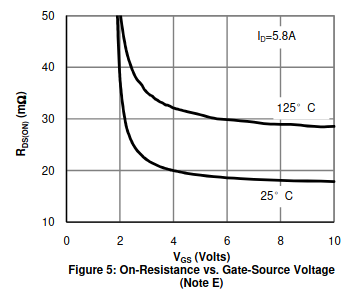
That’s another graph showing basically the same thing, but ‘zoomed out’ so instead of 0-3V and showing Id it’s showing 0-10V and Rds(on), so it’s more explaining the effect of much higher gate voltages.
So, in this case it’s a small FET and we’re not wanting to put much current through it so it should turn on pretty quick.
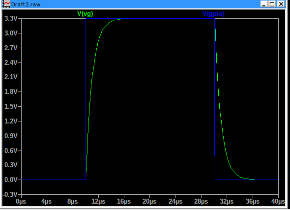
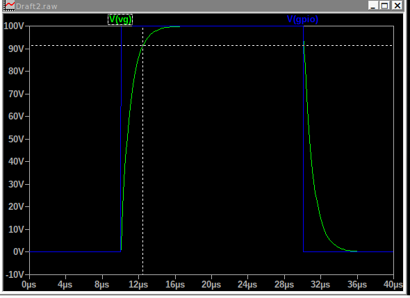
The GPIO pin is driven both high and low so it’ll be the same in both directions, in fact I’ll add that to the simulation…
That’s what happens when the GPIO is high for 20us before going low again. In this case we can see that the waveform is the same just inverted for the 3.3V to 0V case. In fact, because the RC waveform always looks like this, we can actually define that with a single number which we call the step response, i.e. response to a stepped input. That’s typically defined as the time taken to go from 0% to 90%, so with a 0V to 3.3V step it’d be the time from 0V to 3V which is roughly 2.5us. Same as the time taken to drop to 0.3V with a 3.3V to 0V step, which is also 2.5us. Or the time taken to go from 0V to 90V with 100V applied, etc.
Anyway, that’s not too bad. That little FET is connected to resistors that are nearly 100K in total so all it needs to do is get to even 1K resistance and it’s probably on enough for out needs. That happens at a pretty low Vgs so likely it’s only causing a 500ns delay and going from +Vds to 0V quite quickly.
That’s actually another thing to consider, there are 2 aspects to timing issues. One is delay, the other is transition time. Delay isn’t too bad because we don’t care if a PWM signal is offset by a couple of us, as long as it is still the correct PWM and the waveform looks clean. The transition times are what we’re more interested in. Delays do become very important in other situations, though, like communications where it can cause data errors or where it needs to managed to ensure something turns on/off in the right sequence. It can matter where the delay from ‘on’ to ‘off’ is different, too, because if it takes 1us delay before something turns on and 10us delay before it turns off, that’ll change the duty cycle of the PWM, but that’s a story for another day…
So we move to the actual problem at hand, which is the next stage, the P-channel stage. This is the same kinda thing as what we’ve just looked at, but with a couple of wrinkles… We’re not actually driving the gate from 0V to 24V, we’re just driving it one way by connecting the bottom of that divider to 0V using the N-channel FET and then we’re letting the resistors in the divider ‘pull’ it back to 24V. Because of this, we’ve got 2 competing things we’re trying to design for. One is that we don’t want those resistors too low of a value because then when the N-channel FET is on we have a LOT of current from the 24V line. The other is that we don’t want the resistors too high because then not much current will flow to charge the gate capacitor.
So chucking THAT circuit into LTspice, it looks like this:
I’ve used a voltage controlled switch for the bottom side, labelled LowSideSW. Ignore that, that’s just an ‘ideal’ version of the circuit before that’s a bit easier to control. It instantly turns on to 10mR and instantly turns off to 1Meg just for convenience and so it’s not influencing the 2nd part of the circuit. In reality we’d build up a model of the whole circuit but I can’t be bothered to hand-create a MOSFET model for the one you’re using or find an equivalent right at the minute.
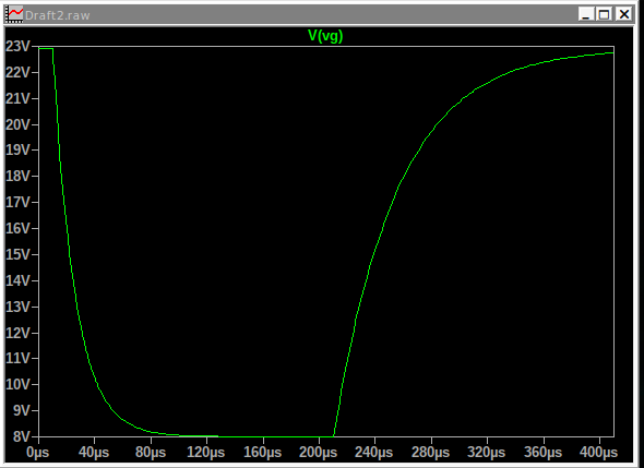
So in that situation, this is what the gate voltage looks like:
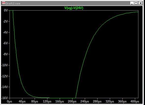
Same thing, turns on at 10us, takes maybe 70us to complete its ‘step’, turns off 200us after turn-on at 210us and then takes maybe 150us to change state back. That’s just the gate voltage relative to 0V, of course, so this is the actual Vgs:
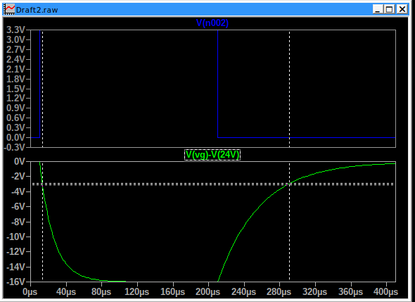
I bumped the switch resistance up to 100Meg because 1Meg is a bit too close to the resistance of the circuit and it was influencing it a little so it wouldn’t go to 0V. So looking at that, we can see how long it’s taking to make those transitions now that it’s the same 1nF gate capacitance but driven by a 47.5k and a 23.8K divider rather than a direct 1K resistor. It makes a big difference. The other thing is that because our Vgs(th) is at -2V roughly, it takes much less time to go from 0V to -2V than it does to go from -16V to -2V. That will cause a significant delay in one of the edges which will change the duty cycle, as well, as you can see here:
The top trace being the signal that controls the switch and the bottom trace being the result.
Then add to all of this that this is still just the gate voltage, not the actual resistance of the FET and the resulting output, it all gets kinda annoying quickly.
Nothing is ever out of the question, or even necessarily ‘that’ difficult, after all we switch 85kHz at 1000V and 250A with no appreciable waveform distortion. It’s more just that it’s a solid step in complexity beyond what you’ve been designing so far. If you think it’s something that’s valuable to have and important enough to devote a little bit of BOM cost to it should be quite possible.
I think you’re also being led astray somewhat by following other designs that are already a little bit ‘amateur’, meaning that in the literal sense, not a pejorative one. The assumption being that hopefully they work fine and don’t have issues but you never know, especially because I still suspect that most people when something goes wrong tend to assume they did something wrong themselves rather than it being just a random issue with a design being on the edge of operative spec etc.
If you’re dead set on wanting 24V PWM there are some options. One would be to do our own half-bridge drive, where it’s both top and bottom switched, or to use something as a high current buffer like a gate driver IC etc. There are ways, it just might take me a week to get enough time to look into it, if you’d like some help there.