It’s tough to tell, typically I wouldn’t just be upping the copper weight on a design, I’d be designing with that copper weight in mind. As I said before, it’ll help with the temperatures by spreading the heat across the board better, but it’s not going to be a night and day difference, I don’t think. More like maybe 5-10 degC, if I was to place a bet on it? Whether that’s worth it in this design or not is one of those typical Product Management decisions that I can’t really help with. It’s potentially a good marketing bullet point, as Gigabyte have found with their motherboards, so maybe there’s that.
The real value with higher copper weights is that you can thin up power traces which can make routing easier/quicker and regain you some board real estate… It’s not by a factor of 2 because we design to thermal rise of a trace. I typically aim for 10 degC for comfort, 20 degC as a maximum if I’m really pushed. Doubling the copper means that if you halve the trace width you’ve got the same resistance so you’ve got the same power dissipation per unit length. The power dissipation of the traces is pretty much entirely based on the surface area of the trace so halving the width means doubling the thermal rise per unit power. So in reality, doubling the copper weight means you can drop the trace widths by about 30%, more or less. I figure all this out with the Saturn PCB Toolkit app but it’s all just based on common IPC graphs so any online calc will likely be ‘ok’. Just bear in mind that it’s all pretty idealized values so margin is a good idea for anything critical.
The other thing to watch with higher copper weights is that the minimum trace and space feature sizes increase. A 1oz manufacturer might be happy with T/S at 0.1mm but the extra etching time means they might need 0.15mm at 2oz and beyond. That’s another reason why I dislike the idea of changing the copper weight partway through a design, it can be a real horrific time sink going back and massaging the layout to hit the right targets. It’s also usually a patch up job which leads to compromises compared to a clean layout from the start. That can eat a lot of the gains you make in smaller power traces, too.
In this case, higher processing cost doubles the price. In high volume the price of the item approaches the price of the raw material. Copper cost is dominant.
OMG I am going to lose my freaking mind. All my sample connectors came to a total of $3.88. With basic shipping and tariffs, they now cost me, and added $73.40.
The prototype boards are so expensive.
I already cut out the MPCNC until prices stabilize. I lost more than $100 on just two shipments in shipping fees because they change daily, So now I suppose I have to start the day checking all the shipping rates before I get started for the two locations.
Wits end, I tell you, wits end.
I am taking a long weekend and I will be sitting at a river, either scratching lottery tickets or panning for gold. One way or another, I will bring the fun back into this so the fees hurt less.
I think that would definitely be worth it. I have a tone of room between my traces so I assume that would be fine. I will wait to test it until I think I have a board that is ready.
I also think I can redesign the box a little bit to provide a air flow path that flows from one side to the other. IF we can get away from heat sinks that is one less thing I need to deal with, if not, I assumed I would need to get them anyway. If every single item is going to cost 19X we need to be real careful of how many items I get.
It’s also trace width that’s an issue, not just spacing. What settings are you designing to currently?
I’d say regardless of the heatsinks, an aluminium mount plate like I mentioned is worth considering. It’s something that’s an additional part of easily sourceable/manufacturable by people individually if they want, rather than the heat-sinks which are simultaneously difficult to hand make and kinda worthless at their jobs
Edit: Also, to reiterate, thicker copper will mean longer times to reach thermal equilibrium so if you’re doing any actual thermal testing, definitely consider how you’ll verify that you’ve given it long enough to fully soak.
Yeah, that’s a decently large feature size. Good place to be if you don’t need to go thinner. 0.2/0.2 is my usual go-to for simpler stuff these days but larger is almost always better in this kind of application.
Just thinking on it further, there’s the possibility of making a 3D printed enclosure that screws down over the top and makes the metal backing plate fully external to the machine, too.
I dunno if I posted the water heater controller I made but that was a 3 piece enclosure where the base was a heatsink then a separate sealed-ish housing got screwed to that and finally a lid to screw on the top. It worked remarkably well and I’ll be using that approach again…
Thinking about it, when we were doing that with our capacitor arrays we couldn’t really use conductive fasteners because of the huge clearances needed for the high voltage. We were using contact adhesive or double-sided tape to fix a layer of Mylar/BoPET in place and then using more contact adhesive or double-sided tape over that to fix the board down. It worked well enough that we used a couple of nylon fasteners for peace of mind but didn’t need anything else.
No issues with just sinking a metal screw through into the backplate here. Without the high voltage needs, a patch of double-sided tape would likely do that perfectly fine. If you want to go fancy there are specifically insulating thermal tapes but with relatively low heat-flux and non-mains voltages I’d leave that as a backup plan.
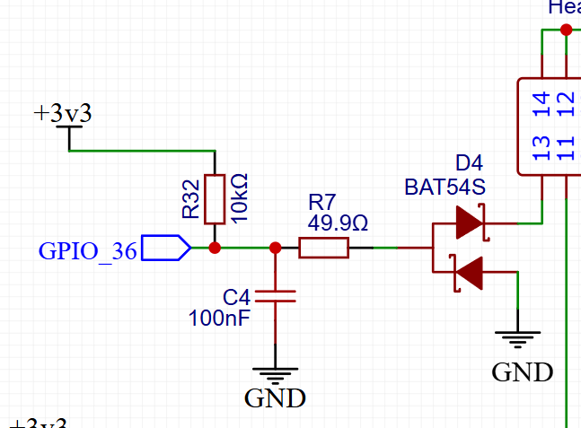
Can you elaborate on that? That barrier diode is really there for ESD protection of the GPIO.
As drawn, GPIO_36 should be pulled up through R32 and only pulled down if you close pin 13 to pin 14.
What is the configuration of this pin in your YAML?