Okay, that worked, boot timing curves look the same as the good ones…but I still need to hit reset to load the webUI.
1 Like
Does that mean its something else that is making you have to hit reset? Seems if the timing curves were the same it should load the same correct?
Well we had this issue before…I “corrected it”. The espressif docs show a boot button debounce cap. That cap does not work. I pulled it off…boots up like butter!!!
So I guess it always booted into download mode, and reset would turn it to regular mode.
1 Like
That was the resistor that we had to add to the early versions and you had installed on later ones right?
All in all, new drivers, new outputs, new 5V ps. I only made a couple little mistakes. I don’t feel to bad about it.
Last thing is to take a minute to think about the power logic
3 Likes
No, I removed the use of that pin all together so we don’t juggle weird flashing issues. This we did have on the jackpots as well but it was the very first thing to remove, I forgot all about it.
2 Likes
The board looks GREAT! I am excited to see how much easier it will be to work with on new builds.
Did you happen to add a plug for the fan to connect to? I know that was mentioned at one point before you started the redesign but wasn’t sure if it stayed lol
2 Likes
Congratulations!
I fly home from Paris today, so will be a bit more available if anything needs troubleshooting.
3 Likes
Hopefully I can get involved in some of this discussion a bit more now that I’m back to having some free time on my hands!
I wouldn’t think that’d be an issue, we routinely cable-tie stuff to PCBs. PVC wire sheath is pretty tough.
I’d be very skeptical… Heat-sinking is all about surface area and going from having a heat-sink to board only is a major change, even with the relatively poor conduction through the stack. Definitely not 7%, more like a factor of 3-4x I’d suspect!
I’d all but guarantee there’s a way to do this. It’s VERY common to have non-PCB BOM items listed with instructions like to have them bagged in sets with each board or to be shipped already plugged into the PCB. I do that with several product lines currently. If JLC cannot do this then that’s another mark in favour of a different supplier, perhaps. Happy to help with that process if you’d like.
I’ll try take a closer look at that when I can and get my head around what’s going on there.
Absolutely, admittedly I’m in a different market segment but I always like to start out with the price high and then lower it over time once I have more of a handle on the soft costs. Dealing with failures/RMAs, updating documentation, fielding questions, all of that stuff takes tons of time and eats into margins. Every hour you spend doing that is an hour you could have spent doing something else, after all! People who are keen and want the latest and greatest will happily pay. If you’re up-front about how the price may drop in future as production optimizes, people will understand. This is how ALL manufacturing works, after all, it’s just that people get used to not seeing it because big companies eat the low/negative margins at the start and keep prices high later in the lifecycle to balance it out.
Entirely up to you. Think about it from first principles. They make the board WAY easier to work with and far less error prone if you’re changing components or diagnosing things but they’re not magic. I have plenty of designs where the designators just don’t fit or need to be remote, which makes them less useful. I have a couple of designs where huge sections of the board don’t have designators and we need to use a separate component map to deal with them. That’s frustrating and more error prone if you’re needing to work with them directly but zero issue if you’re not touching it and the design is mature. There are also halfway points like hiding designators for things that are obvious and don’t need them, such as in your example: CARD1 (which I’d never use as it looks awful ![]() ), U14, D1, decoupling caps like C28, C65, C66, etc. Also, presumable that chip needs more decoupling than is shown
), U14, D1, decoupling caps like C28, C65, C66, etc. Also, presumable that chip needs more decoupling than is shown ![]()
Oh well, comments are valid for future situations, anyway! ![]()
How long were you there? Sounds like you, me and someone else on the forum may have almost overlapped!
5 Likes
Thank you for taking keeping an eye on this thread. I don’t mind fumbling around a bit and forcing myself to learn some things. You all are teaching me so much, and have already taught me so much, I was much less nervous going into this one.
3 Likes
8 days in Orléans.
I’ve lost lock here.
You had some kind of weird 3.3 / 5V issue. Something about VMOT also?
What open questions do you have at this point? I’m still willing to pay for some release candidate boards if you want me to put some run time on them.
1 Like
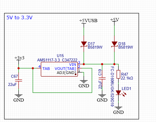
USB +5V → 3.3V regulator ← +5v from Vmot.
The 3.3v feeds everything. I just needed a diode from +5v from Vmot so I do not back feed the the 5V PS.
The only question I am not 100% on is if Vmot is powered and the USB is plugged in both will feed the 3.3V regulator at the same time. There is no issue with that right?? 5v is 5V it will take from either/both.
Normally the ESP32 devkit has the 3.3v on board and we only diode the incoming 5V, this needs both.
1 Like
At a high level, not really. If you consider the diode ideal (fixed voltage drop regardless of current) then whichever voltage is higher will supply the current and the other will be effectively disconnected.
With a more real world consideration of the diode (forward voltage is relative to current and ramps from up from zero volts at very low current levels) then you’ll get some current sharing based on the voltages of the supplies, which is worth considering. For the same configuration you could have effectively 100% from the USB, 100% from Vmot regulator or a mix in between.
I don’t think there’d be an issue with this. The main thing to be aware of when putting diodes in line with supply rails is that your 5V is no longer 5V, it’s 5V minus the diode drop at the rated current. I can’t offhand remember what the current draw from the 3.3V line was being sized for but assuming it’s ~250mA then you’d go to the graphs on the diode datasheet and look at what Vf is at If.
At 250mA it’s around 0.35V so you’d then calculate what the minimum input voltage to that regulator is. I usually consider voltage rails as +/- 10% unless otherwise specified but for something supplied externally like USB with unknown power supplies and cables, I’d consider that it could be even lower depending on load. Ignoring those aspects for the moment, at a nominal 5V we’d end up with 5V - 0.35V = 4.65V after the diode. That’s already a little close to the dropout voltage of the AMS1117 (1.3V max at 0.8A) so having that diode there it’s worth considering that your +3.3V rail will have the potential to sag under load. In reality, the drop-out voltage will be less than that at lower currents but there’s no info in the datasheet to go off, although the 5V rail will have tolerance as well, so it’s a bit of a crapshoot…
This is why I’d normally try to find a better quality regulator for that job, which I think we’ve previously discussed. 5V to 3.3V with a linear reg can be a little tight. TI has some
Alternatives to that are to simply live with the 3.3V varying and just hoping for the best, considering that variation downstream and making sure it won’t upset anything else, using a regulator with a lower drop-out voltage, using a higher voltage to supply the regulator, checking enough of the AMS1117 parts under actual load to be somewhat confident in their specs at actual target current…
1 Like
Yeah I double checked those. The 5v to 3.3v can take a wide range of input so that part seems safe.
I will triple check the output. My 5v was 4.93+ on all boards, and the 3.3 was 3.31 on them. So I think it is good but I can fire it up again and check everything under load as well. Just need to solder the diode in place first.
Thank you!
2 Likes
Just to clarify a bit further, it’s not the input range I’d be worried about, it’s the dropout spec:
![]()
That gives the minimum voltage needed between input and output to maintain regulation. So if you’ve got 0.8A coming out of the regulator, you’re going to ‘lose’ 1.1V typically across the regulator… So that’d be 3.3V out, 4.4V in, minimum. Spec is only guaranteed to be 1.3V so 4.6V to never have to worry about it. It’ll likely be lower voltage with lower current, but with no information provided by the datasheet, it’s tough to make a call on how much that’ll actually be…
If you have less than that then typically the output voltage from the regulator will sag a bit below 3.3V but it will also start to be modulated by the load current, so if you get a big pulse current draw the voltage will sag further, etc. That’s generally best to minimize as it can cause other unexpected secondary effects.
2 Likes
Okay so we need to be specific about the 5V outputs capabilities to prevent that, which is only during Vmot power ( we have 3A and a extra 100uF cap). USB power only runs usb and the esp.
1 Like
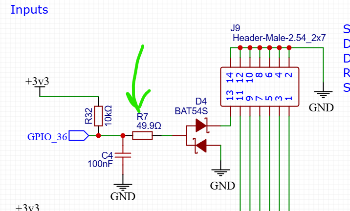
This value is not doing anything critical is it? If I can go to a 47.5ohm I can eliminate a BOM Item.
Short answer:
No issue with that change. Always a good idea to try to land on values from the E12 series like that, where possible.
Long answer:
The way that component is selected is that it’s primarily creating a low-pass RC filter with C4, so changing it will change the cutoff frequency of the filter. For filters like that, the actual frequency isn’t usually critical. Typically you’d either think of the frequency if it’s an AC or pulsing signal coming in, or the rise time if it’s a edge trigger like an end stop or on/off line.
There are a ton of on-line calculators for that etc. My favourite is:
http://sim.okawa-denshi.jp/en/CRlowkeisan.htm
If you plug in 50R and 100n it shows the corner frequency as 32kHz and a step response of 11us. So I’d look at that and think to myself that an instantaneous signal change will take around 11us to make it through the filter to the microcontroller and that any frequencies over 10x the corner frequency, so 320kHz, will basically cease to exist in any meaningful way. That’s naturally a ‘little’ simplified, but not too much. Technically you’d consider the effect of the 10K pull-up as well, but there’s enough difference here that it’s negligible… If you’re interested, I’ll explain how to calculate it properly sometime! ![]()
Because of the diode, that step response only really counts in the pull-down direction so then the next thing is to consider the same thing in the opposite direction. It’s a 10k/100n in the rising-edge direction so you can use the same tool to get the step response with 10k/100n and it’s 2ms. So in general, 11us to respond to it being externally pulled down, 2ms to respond to it being released and being returned to a high state by the pull-up.
The final part of it is the voltage states under the 2 conditions. With the switch open and the line floating high it’s reasonably simple, it’s just the 3.3V rail and the 10k resistor. Technically you’d look at the bias current for the input which is how much current comes in/out of the input in different states, but that’s usually low enough that you don’t need to consider it for a 10K pull-up, maybe 100K+ you might. For the switch closed/low state then you’d consider it as a voltage divider being created by the 10K and 49.9R resistor, with the latter connected to 0V. Again, that’s enough difference that this isn’t ‘really’ worth doing, but for the sake of argument we might as well. I do this by adding the two, so it’s a 10K + 49.9R so 10,049.9R resistor and then working out the current through it. 3.3V and that resistance leads to 328uA. Voltage would be 16mV, total power in the divider is around 1mW. Both completely negligible in this case, but still useful to specifically consider.
I often put some of these numbers on the schematic as well to make it easier to review and remind myself what the parts are doing in the future. Typically the frequency response and rise time, at least. Power in any resistors that it might be getting close to ratings or important, etc.
That sounds like a lot, but I usually do that in a spreadsheet for each design I’m working on so that I can easily document it for the future, do a couple of versions of each, see the effect of changes easily etc. and add extra calculations to anything that is needed. When adding another section it’s copy/paste a previous design section and add it in to a different part of the sheet, etc.
Something like this:

So I can easily see that it’ll barely change anything.
Edit: Usually with a screenshot of the circuit itself next to it so I can refer to the actual designators because sometimes it gets quite a bit more complex…
2 Likes
This is a classic case of the more I know, the more I realize I don’t know. There are so many layers to this onion for basic circuit design. I can not imagine what happens when faster response times are needed.
I am just learning about heat ratings and probably 3 out of 20 specs on the sheets.
Heck I finally understand what an inductor does (seemed a lot like a capacitor for a long time…then I learned time gets factored in).
2 Likes
Aint that the truth! ![]() I spend a lot of time with that exact same feeling, honestly.
I spend a lot of time with that exact same feeling, honestly.
Yeah, in power electronics we often live or die by thermal ratings. We use a simulation suite called Plecs that allows use of highly detailed thermal models that take into account the thermal mass of various parts. So when the datasheet says something like 0.5 degC/W junction-to-case, that’s fine for steady state but what about when we’re halfway through a 900V/250A switching transition and dissipating ~240kW instantaneously? It only takes ~20ns to make the entire transition so it’s not ‘that’ much total energy, but it’s still gotta go somewhere. Using the thermal models provided by the manufacturers we can see the die temperature briefly heating by 10 degrees over that 20ns period and then cooling back down in the ~10us before the next switching transition. That’s an important detail when you’re trying to figure out how close you are to thermal limits!
That’s not including the difficulties with predicting behaviour of heat-sinks over time because they’re always extremely poorly specified. I could probably give a several hour impromptu seminar on thermal issues in electronics ![]()
Yeah, although that’s often the situation. You’ll likely find that you can do 50% of the design with with 2-3 specs, then you’ll run into an issue and get it to 75% fully designed by considering 1 or 2 more, than 90% with another one etc. It’s unlikely that there are any situations that need to take into account every spec in the datasheet, there’ll usually be a few that are critical for your application and a bunch that can be safely ignored. The real fun starts when you realize that some of the information you need for certain scenarios isn’t even in the datasheet or may just be blatant lies… That’s a common situation in EMC/safety applications, sadly.
Inductors are by far the most complicated passive to get your head around so that’s pretty understandable. The bad news is that they’re also probably the component where they’re both the most poorly specified in datasheets while having the most significant difference in real-life performance vs their ideal theoretical performance. The best advice is to not use them unless absolutely necessary ![]()
4 Likes