I guess it doesn’t matter hugely but finding a spot for a ground test point would be a good idea. Doesn’t need to be populated. I usually get one board back for bring-up and fully populate all the test points (often ~30-40 of them), then have the initial testing boards with a few key ones, then just leave them off for production.
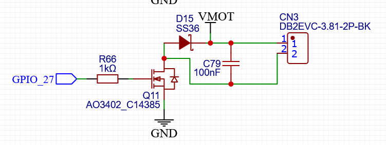
Is it loaded? Did you move the capacitor off the +Vmot to Drain? Actually, I think I’m looking at an old version of the schematic perhaps?
I’m not sure what you mean by this. I think your ground connection is fine, I would just add a specific ground test-point somewhere for the probes deliberately for testing.
Something like the Keystone loop test points I mentioned a while back.
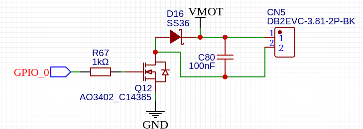
That’s what it should look like. The cap is there to supply the in-rush current from using the switch on a load that has capacitance. Some of the current will then come from the Vmot side of the cap, through the Vmot connection to pin 1 on the connector, into the load, back via pin 2 of the connector, through Q11 and then through the GND net back to the GND connection of the cap.
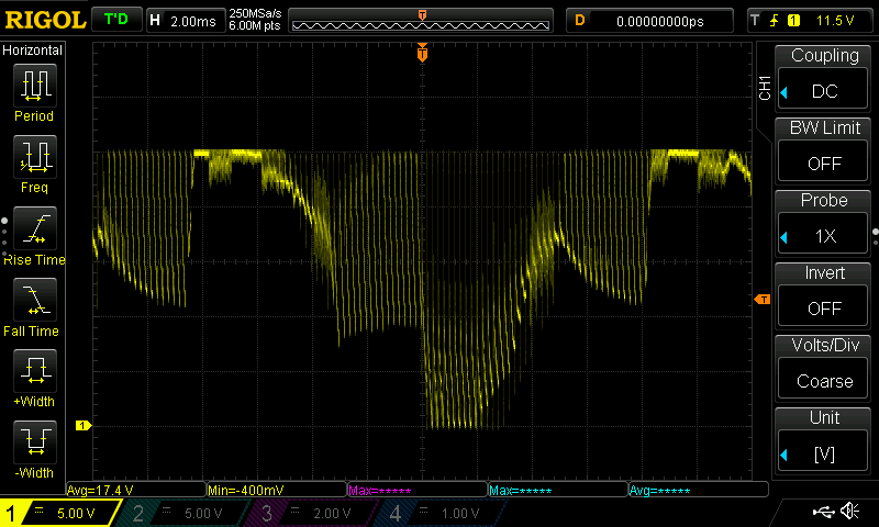
The way it’s drawn currently, every time you turn on the switch, it will need to charge that capacitor which will slow down the turn-on voltage rate and pull a spike of current out of Vmot. Any time you turn off the switch it will start discharging the capacitor before the voltage changes. If you’ve got a pretty big load, it’ll switch off quickly because 100nF isn’t much energy. If you’ve got say a 10K resistor across it, the step response equation comes back again. It’ll look exactly like the turn-off edge from your digital waveform above but instead of being 330ns it’ll be 10K/100nF which is more like 3ms…
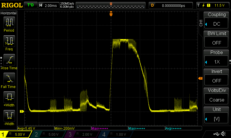
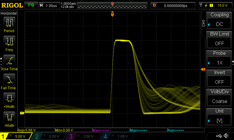
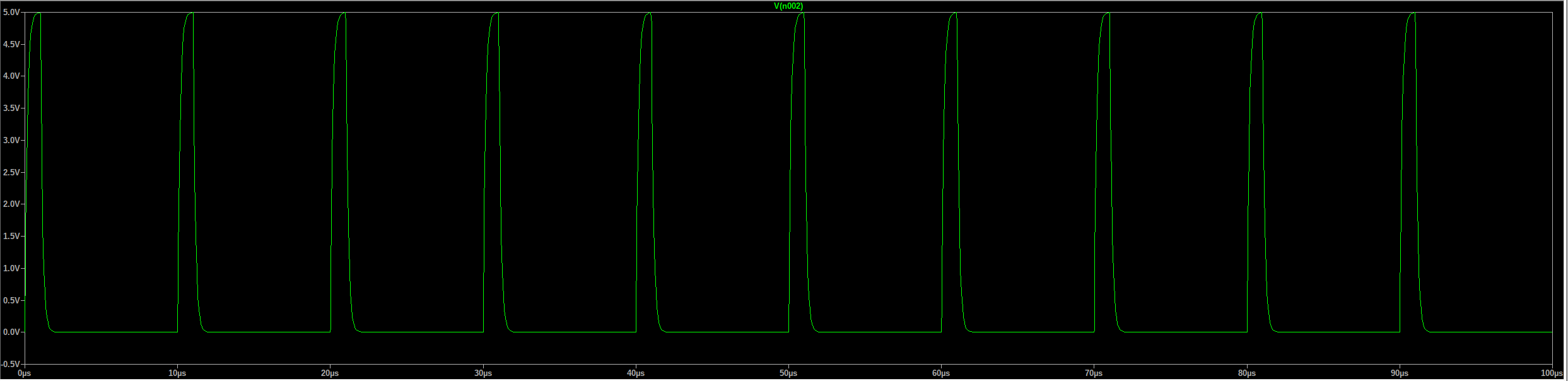
330ns should be shitloads for a 5kHz PWM… That’s 1us/div so that’s a 1us pulse. 5kHz is a period of 200us, so that’s a 0.5% PWM? Yeah, that’s always going to look like garbage… Try it with 10% duty cycle.
Eh, I don’t really like ‘filter out the noise’ as a way of thinking about it, it doesn’t really do much to actually understand what’s going on and can lead you down the wrong path.
All noise is just voltage or current signals where they’re not wanted (kinda like how weeds are just plants growing somewhere you’d rather they didn’t). In general, capacitors provide a low impedance path for currents so they can flow in a loop without creating unwanted voltages. Resistors provide a high impedance path so that voltages don’t provide unwanted currents, etc.
Having the capacitor across the terminals of the switched output will mean that any current pulses or higher frequency signals (‘noise’) from the load you’re switching are able to return immediately to the load rather than making their way elsewhere into your board, so that’s good, but at the downside of the switching action then causing you to suddenly place a discharged 100nF capacitor across the +24V which will create its own unwanted pulses of current etc. Having the 100nF outside the switching loop but next to the connector/FET means that it’ll still provide a bypass for the unwanted currents but without needing to be switched which causes its own issues.
I don’t know what you’ve configured it as, but that’s not relevant. The pulse width shown by your scope is 1us. The period, if it’s meant to be 5kHz is 200us. That’s a 0.5% duty cycle.
Most PWM signals will have a minimum and maximum bound on the PWM for this exact reason, it starts to distort (aka look like crap). It’s not uncommon for things to be specified as running 0%, 10-90% or 100%. So basically avoiding the 0-10% and 90%-100% by rounding to the nearest option and avoiding the partial turn on pulse like you’re seeing.
Either way, I think that’s a perfectly acceptable, even quite good, 0.5% PWM at 5kHz. The answer is if you need 0.5% duty cycle, reconsider what you’re trying to do and do it in a different, better way.
That’s the same circuit at 100kHz/10% duty cycle. If you wanted 100kHz PWM bandwidth then I’d probably speed it up a little, but not by much.
Bear in mind that the outputs before had zero filtering components. They’d probably run into the 10s of MHz if you wanted. The key thing to note is that that isn’t a good thing unless you actually need that bandwidth. If you have 10ns switching edges then sure, you can run 10s of MHz of bandwidth but just because you’re switching it at 5kHz it doesn’t mean anything, those edges are still there. And the faster the edge, the more likely it will couple into other signals or cause other issues. So you might get nice crispy looking 5V PWM waveforms (which mean absolutely nothing in practice), but you might pay for that by having it corrupt the comms on the pendant if the wires are routed nearby, etc.
The other thing is that circuits that can produce fast edges will also necessarily be circuits that are susceptible from interference from fast edges. So a high frequency signal, say from someone keying a walky talky near the board, could couple in via the lines connected to the output, couple through the FET into its own gate and turn the FET on briefly, or pull the gate voltage enough that it causes damage etc.
The whole approach of defensive EMC design is that you try to prevent issues before they occur, largely because you can’t predict when they’ll occur or even know for sure that an issue you’ve run into is an EMC issue. Hell, you may have seen people with broken outputs on their boards or other issues that are caused by this, you never know. For this reason, you try to make signals only as fast as they actually need to be. If you want 10kHz PWM at 10% minimum duty cycle, 100-500ns is a perfectly fine rise time. If you need 100MHz signals coming out then you do that in other more complicated and expensive ways (differential drivers, shielding etc.) because the cheap, easy, good and reliable option is no longer available to you.
So this happens even if I touch the USB ground from the cable to the board. Computer issue, ground stuff going on? It is not the actual USB just the grounds getting connected.
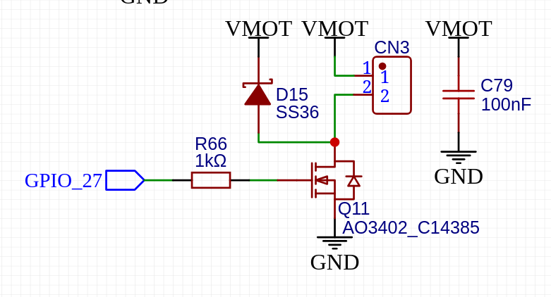
Have you removed the 100nF cap across the terminals of the connector? That needs to go. ASAP.
Heh, yep, probably. You’ve probably made a semi-resonant circuit with the parasitic inductances and the 100nF capacitor.
With the cap gone, any level of resistance should make that edge look a lot cleaner.
But also, what were we wanting high frequency PWM on that output for, again? I thought it wasn’t for the lasers or spindle control because they needed it to be 0V referenced, not +24V referenced?
What’s your computer connected to? If it’s a laptop and just the power brick then it might be entirely floating/isolated, which means it may be charging up a little. When you connect the ground of the laptop to the ground of the circuit it will be discharging. It may be that the +24V isn’t moving at all, what’s happening is the 0V reference of the scope is dropping, so relatively speaking it ‘looks’ like the +24V rail is changing voltage.
If that’s what’s happening, it’s like trying to measure someone’s height while you’re standing next to them but you’re on a trampoline. If someone else jumps on next to you, it’s going to look like that person suddenly got taller, which would be an insane conclusion to draw when what actually happened was your ground reference (the trampoline surface) moved out from under you.