Jackpot V2

That’s a topic that gets really complex. I’ve read so much conflicting info on it that I’ve kinda given up. I just put a 100nF X7R capacitor with a voltage rating at least 2x what it’s expected to see on each pin and call it a day. If it’s a power supply pin then I’ll do a 10uF version of the same thing, usually in a 1206 package as well.

That comment was about putting the decoupling cap on the ‘power’ pins of the ESD suppressor, though, because it’s the type that has an internal diode bridge that directs energy into the rails, as well as its internal TVS.

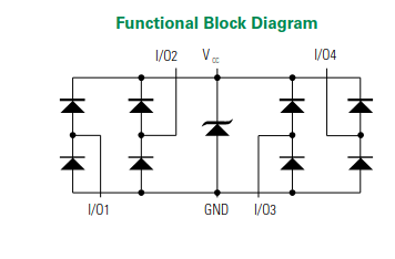
This is the type that I suggested:

Each IO pin has a diode to Vcc and a diode to ground. That’s basically the same structure that’s in the ESP32, just that it won’t be designed to handle a lot of current because they’re trying to cram a ton of other stuff onto that die and using tiny structures in order to keep the die size and subsequently costs down. In this device it’s designed to take much higher pulses of current specifically for ESD strike situations, although it’s still relatively small as protection devices go as can be seen by it’s 4.5A rating, it’s a ‘bit extra’ protection, not anything super bombproof.

So when the ESD strike occurs, it’s basically the same as having a tiny capacitor charged to several kV connected directly to the incoming pin. With no protection devices that voltage will get applied directly to the ESP32 and lead to a lot of current flowing where it shouldn’t, burning out the pathways on the chip.

These devices work by redirecting that energy elsewhere, ideally before any of it gets to the ESP32 but in reality more like sharing it out. With a plain TVS is is basically just a big zener diode with a crappier datasheet. Assuming a positive ESD strike, the one you posted above will do nothing until the voltage gets to around 16V then it will start conducting. As the voltage continues to try to rise it will start conducting more with its terminal voltage rising accordingly until it sees ~18V at a few amps or whatever. Depending on how serious the ESD strike is, the current will keep rising to a point and then start to drop back as the capacitor is discharged into the device. The TVS is just there to try to reduce how much of that ~10kV actually makes it to the ESP32 or other devices, or even the circuit board traces themselves. You’ll never actually see that 10kV because things will start to break down and conduct before that, which makes the explanation difficult, but if the TVS was soaking up 4-5A at 20V then if it wasn’t there that same current would have to go through the ESP32, eventually. The TVS is designed to handle that, though, and so it survives, just getting a little warm in the process as the energy is dissipated in the lossy semiconductor junction.

With the diode bridge style then ideally they’re connected with the Vcc and 0V pins to your rails. As the ESD event happens and the voltage starts to rise the diode between the IO pin and Vcc starts to conduct and essentially ‘clamps’ it at Vcc. For a small strike and low current that might keep it to Vcc + 0.5V, let’s say. For a larger strike there will be more voltage between the IO pin and the Vcc pin but it also starts to depend on what happens to the Vcc pin. Maybe it ends up going to Vcc + 2V at 4A, let’s say. The next part of that is where the energy goes because all that diode is doing is steering it to the Vcc connection. If there’s nothing else connected to the Vcc pin then the internal TVS will start to conduct and the voltage will rise to 11V or so. If the Vcc pin is connected to the voltage rail then the rail itself will start to rise, charging the capacitors. An ESD strike has a lot of voltage but not actually that much energy, fundamentally. It just delivers it very fast and in such a way that a lot of bulk capacitance like electrolytic capacitors won’t be able to ‘keep up’ and respond. That’s why having a decent high-frequency decoupling cap on the pins is a good compromise, it’s not so much energy that it can entirely swamp the ESD strike but it’s fast enough that it can respond and absorb some to limit the voltage rise further. The other nice thing about having the strike redirected to Vcc is that it can cause Vcc to rise slightly during the event which also helps to protect the IO pins. Usually the damage to the IO pins is because of them exceeding Vcc and causing parasitic conduction within the die. If Vcc rises along with the IO pin then this doesn’t happen. Of course, that puts you at risk of damaging the entire chip with Vcc getting too high but that’s less likely given the limited energy of the ESD strike and the number of decoupling capacitors around the place.
2 Likes

I guess I am not really sure what we are trying to protect against. This is a covered socket on both ends, how often is this going to get hit with ESD, and it can’t get wired or plugged in wrong.

Is Bart’s method okay, do we need any at all, what do I do here? The clamping voltage is making zero sense to me. I can’t find any clear documentation on design guidelines, I am not seeing any diode bridge style classified as ESD protection. We are clearly in the advanced section of EE now.

1 Like

It’s not just about the expansion socket. The pendant get plugged and unplugged. Sometimes people do the plugging/unplugging hot. The cable potentially hangs out on a beam alongside an ESD generator (dust collection hose). People touch the contacts of the pendant cable with fingers in that same potentially charged environment. Plenty of opportunity for events. Not just ESD. Inrush/outrush.

3 Likes

Half joking… Consider adding bare minimum components needed to make the board qualify as a cellphone, to qualify for tariff exemption (for this week at least).

Does (or could…) JackPot v2 qualify as a tariff exempt “Embedded Control Computer” 8471.80.1000 or “Educational / Robotics Controller” 9023.00.0000?

It has wifi and bluetooth, maybe it qualifies for a different HS code that is less expensive. I thought all HS codes were affected now though. I find it actually pretty hard to find up to date info on this stuff.

Seems like both are plausible, are they taxed favorably?

2 Likes

So, the short answer first and then there’s a lot of waffle below:

If you know it’s an issue but don’t have enough information to mitigate it (often the case with these more advanced issues) then you do the best that you can in the initial design stage and adjust the design afterwards in testing. This is why you’ll see lots of components that aren’t populated in commercial designs, they’ll add a ton of filters for EMI, protection for surge/ESD, etc. to start with and then spend a week in a test chamber figuring out which ones can be removed safely. If you’re good/lucky then that’s how it goes. If not then you start scrambling to figure out how to add what you need after the fact. If you open a design and see a blue-wired on device or a bunch of ferrite cores awkwardly stuffed everywhere then that’s likely what happened.

In this case, just putting something there is fine, I frequently work back from ‘what’s the best I can do here’ and protect something as much as I think I can get away with, rather than working forwards from ‘what do I actually need’, especially because ‘need’ is often poorly defined.

If you’re struggling, I wouldn’t be looking for diode bridges, I’d look at ‘esd suppressor’ or ‘esd array’.

There’s a thing called ‘machine model’ ESD which is a lower voltage but higher energy strike that can occur when things are plugged in together while not grounded. Someone holding a pendant and plugging it in could easily be the cause of an ESD event.

Bart’s method is VERY coarse and I wouldn’t expect it to do much, honestly. It’s a lot better than nothing but I don’t know how realistically it would solve anything. Part of the issue can also be that this is a whole system situation, changing the micro or even the layout can make the situation better or worse. It also sucks because ESD damage isn’t just ‘it died’. It could be the pin working fine as an output but the input being dead, or going leaky, or going high impedance. Or even potentially something else on the chip dies, I really have no idea. I’ve just heard the horror stories!

Anything in particular that isn’t clear? I’m always happy to answer questions, makes me feel less like I’m delivering a lecture into the void! :slight_smile:

In an ideal world, the clamping voltage would just be one number and the device would clamp any amount of current at that voltage. If we had a device that clamps at 10V then once the voltage rises to 10V it will start conducting and will conduct enough that it keeps the voltage at 10V. That current could be 1mA all the way up to hundreds of amps, potentially, but it’d never exceed 10V. Then what you’d do is take a look at the device you’re protecting and make sure that it can survive 10V for the period of the event. If it can’t then you’d add more protection or filtering until it could, or specify something with a lower clamp voltage etc.

In the real world, though, all devices have resistance and other non-linear characters, so you can think of it like there’s a resistor in series with the clamping device. The more current that flows, the high the voltage that it ‘let’s through’. I guess an analogy could be a pressure relief valve on a boiler. If it’s a low power boiler and a huge valve then as the pressure gets too high the valve will open and the pressure will vent off until the valve closes again. If it’s a high power boiler and a tiny valve then the pressure may keep building and building because the boiler is producing more steam faster than the pressure valve can vent it. It’s helping, but it’s not a hard cap, it’s creeping higher and higher over time. Not a good analogy, I guess. Or a pressure relief valve that has a long pipe attached. Small amount of hot water released as over-pressure and it’ll be at an accurate setting. Lots of hot water released and you’ll start to get back pressure from the pipe, leading to the actual pressure the vessel is capped at being higher and higher, depending on the amount of venting needed.

As for what we need that voltage to be, that’s where good documentation helps, along with potentially a bit of iteration, testing and most importantly in my opinion, a view to a design as being something that evolves over the lifespan of a product, not something that is frozen at a fixed point in time.

Worst case, all you’ve got is the absolute max ratings of a part, but often those aren’t really that useful or can be misleading. The best case would be an application note with necessary protection details or a specification for short term over-voltage or input current. If you know the peak input current then you can work backwards from the clamping voltage and the impedance of the pin under those conditions or add some series resistance. If you know the peak voltage then you can add some filter based on the event pulse shape, etc.

Relatively, yeah. EMI protection and product robustness issues are the type of thing that every professional designer will need to contend with but I’d say 95% of them have no formal training or even deep understanding of the topic. Myself I feel like I’ve barely scratched the surface of the topic even though I’ve been grappling with it for years and have done several dedicated training courses on the subject, the last being a full week event that I had to fly to, delivered by a guy called Keith Armstrong who is kinda one of the fathers of the entire discipline, which I was very grateful to be able to attend.

Why are we not using a 5V clamp, since that is the “max” the IO can handle. Or for that matter 3.3V since that is what we should use?

I’m in the ESD section, ESD and Surge Protection (TVS/ESD) | Electronic Components Distributor | LCSC Electronics sorting is funky but, I know we want bidirectional, and I have tried a few clamping voltages.

1 Like

The clamping cutoff isn’t clean like that. There’s a spec called standoff voltage, working voltage or operating voltage etc. That’s the voltage that the part is designed to protect. At this voltage the part won’t be conducting at all so it won’t be causing extra loss or signal integrity issues. There’s usually a maximum leakage specified at this voltage.

Then there’s breakdown voltage, which is where the device starts to conduct at a relatively uniformly specified test current, usually 1mA but sometimes higher or lower depending on the device voltage. This is where the device is just starting to clamp, but 1mA is so low that it won’t really be doing much protection here.

The next is the max clamping voltage which is usually specified as the point where the device has reached its power limit for that given waveform. This will be a combination of voltage @ current where both of those are specifically tested for that individual part.

For example, the SMCJ series are parts that I typically use as my big grunty input protection TVSes. So looking at the 5V version of that:
Vr = 5V - So at 5V it will be leaking a max of 800uA, which is a little bit high but survivable.
Vbr = 6.4V to 7.0V @ 10mA = So with 10mA through the device, it will be at somewhere between 6.4V and 7.0V. This is where the clamping starts but is still low enough that it’s not really doing anything.
Vc = 9.2V at 163A - This is the max clamping so I know that worst case, as long as less than ~163A is going through the device, my input will see less than 9.2V.

This is a silly example because you’d never use that device for this purpose, it has something like 10nF of capacitance that varies with applied voltage, so it’s very much more intended for voltage rails, but that’s part of what you’re speccing.

So from that you can see that a part that is suitable for use with a 5V IO isn’t going to clamp at 5V, it’ll clamp at more like 7V-9V or more. That’s not ‘that’ bad, because most absolute maximum specs are kinda misleading. For instance, the reverse voltage spec says anything more than say -0.5V vs the 0V pin is maximum, but the thing is that there’s a diode from the pin to 0V that will be forward biased, so what they’re really saying is that you shouldn’t put enough current into that pin to drag it lower than -0.5V. If that’s 10mA to cause damage then if you had a 1K resistor in series with that pin, it could go to -10V and still be fine, because the on-board diode is doing the clamping and the actual voltage at the pin will be -0.45V or something.

This is where the diode array style ones come in. Rather than relying purely on the somewhat poor and ‘slushy’ specs of the TVS, they use the voltage rails themselves. Rather than trying to dissipate all that energy as heat, instead it re-directs it into the voltage rails to be stored in the caps, to be used by other devices and then to be absorbed by a TVS if necessary. This has the advantage that the TVS isn’t connected to the pins unless there’s a high voltage event, so you don’t have a huge capacitor connected to the pins. It also means that the effect is distributed a lot more which can minimize it somewhat. A pin being at 9V while Vcc is at 5V is very bad. A pin being at 7V while Vcc is at 6.3V is less bad and much more survivable.

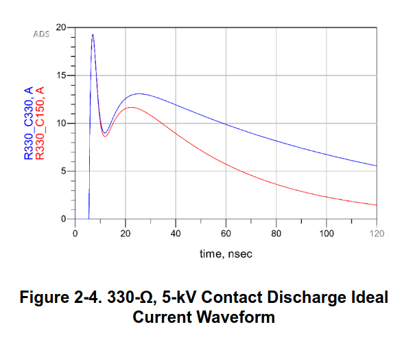
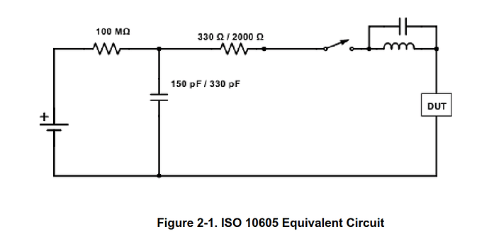
The thing is, you’ve gotta know the waveform of what you’re protecting against. That’s why there are standard ESD/surge/EFT etc. test waveforms, they’re intended to give you a relatively easy way to evaluate your designs without needing to rub a balloon on a cat or roll around on a carpet. ESD is usually defined by a circuit model, such as this one for ISO 10605 which is an automotive ESD standard I’ve looked at in the past.


The ‘battery’ on the left in this case is charged to whatever test voltage is applicable, could be 5kV, 12kV, 20kV or worse, depending on how stringent the testing is and what the expected use case is. The switch is deemed to close instantaneously and without bounce at the time of the strike initiation. It’s also done at least twice, once with positive voltage relative to 0V, once with negative.
The standard resulting test waveform is something like this:

So a few ns rise time and then 100ns fall time. That’s pretty fast, with broadband frequency components well into the 10s of GHz range. That’s why sparks make such good interference generators. That also means there isn’t much actual energy there at all because it’s over so quickly, hence why directing that energy into the voltage rail works well.

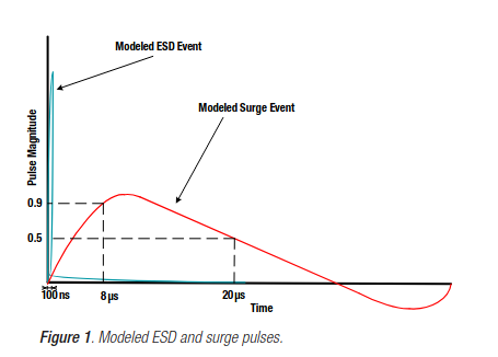
For something like a surge event, that may be an 8/20 or 10/1000 waveform, which is rise time/fall time in us.


That’s from a TI appnote showing the difference in speed between an ESD strike and a 8/20 surge waveform. The surge has much lower peak voltage but MUCH higher total energy and is usually more destructive on a systematic scale. That’s something you won’t see in this situation, but is a consideration for anything connected to cables that run between buildings or are connected to the mains. Typically they’re caused by lightning discharge currents causing huge ground lifts even many miles away from the strike area.

Why do you want bidirectional? Typically that means protecting at voltages that are +/- respect to 0V. Here we want unidirectional because it’s 0V to 3.3V. Actually, you know, I never considered how misleading that labeling was until now… The unidirectional doesn’t mean that it doesn’t protect in the opposite direction, it just means that it’s a simple diode clamp, which is a lot better.

Bidirectional would be for things like ethernet, RS-485, actual RS-232 UARTs, speaker outputs etc. Things where the signal can be both + and - with respect to our 0V reference. Unidirectional for everything else, like voltage rails, GPIO, TTL UARTs, I2C/SPI/whatever.

Edit: Also I truly fucking despise LCSC’s website. I’ve been trying to use it to find something equivalent for a minute and it has eaten my search results 4x and displays nothing useful. Man, designing stuff this was would be tough. I’d STRONGLY urge you to consider how much time you waste trying to use tools like this.

2 Likes

Ah found one!! USBLC6-2SC6 | ST | Price | In Stock | LCSC Electronics

And another, USBLC6-2SC6 | TECH PUBLIC | Price | In Stock | LCSC Electronics

Now lemme read that. yup, unidirectional.

1 Like

I fully understand. A lot of the search is really bad in english.

1 Like

Yeah, there you go. Anything specified as low capacitance is a good bet, not because we need that spec necessarily (although at 1Mb, we probably do need it), but because that directs you to that style of suppressor.

So, key things here:
Specifically says ESD, which means it has low inductance and good response time, necessary for the ~1ns rise time that ESD events can have. For this reason you MUST route traces through this part, you can’t just put it off to the side somewhere. Traces should go from the landing points to the pins on this part and then onwards to the rest of the board. It should also be as close as is reasonably possible to the landing point, really. Actually, looking at it there’s an example of that on page 5.
Peak protection is 15kV discharge both air and contact. That’s pretty good, I’d be perfectly happy with that for this situation.
Clamping voltage - Max 12V at 1A. That’s quite a high voltage but that will be just this chip in isolation. You can add a gruntier TVS or more capacitance at the Vcc pins, or connect it to the Vcc rail, and it’ll do better.
Another key point is that this isn’t the only ESD protection, the ESP32 will have its own internal ESD protection. This is just to make sure that it’s not seeing the full 15kV strike, which means that the internal ESD protection will see less stress and it’ll be much more likely to survive the dramatically smaller resulting strike. The absolute maximum ratings will also be misleading because they don’t have a time component, so you can’t say for sure what the actual pin will survive, short term.

Figure 15 on page 8 shows another great ‘defense in depth’ approach to ESD/surge protection. They have an external bidirectional TVS that’s protecting the transformer, then the transformer itself, then the TVS array, then the data transceiver will have its own internal protection. These things often end up being a bunch of parts all designed and intended to work together, either protecting against individual situations or each providing a layer. A big differential mode surge on the line will get somewhat clamped by that TVS which will stop the transformer being burnt out. The transformer might saturate and not let the whole pulse energy through. The energy that does get through gets directed to the rails by the ESD array. The energy leftover from that gets absorbed by the transceiver and stays within its limits.

1 Like

Even if you start using Digikey to earmark half a dozen parts and then find equivalents on LCSC, that’s what I’d be doing. That part you’ve found appears to be an ST part and then the subsequent knock-off which has a decent chance of being made in the same factory :expressionless:
The ST part would be findable on Digikey and then further searching would lead you to the low price Chinese option. You probably won’t get the lowest of the low, price-wise that way, but think about how many boards you’ll sell over the design’s lifespan. If 1k boards would be great, then I’d budget MAYBE 10 minutes per $0.01 saved. I’d be looking for savings in the $1-2 range first and then moving on.

It’s pretty common to have someone whose job it is to do a BOM review and flag parts that may be opportunities for cost reduction, issues due to single-sourcing or part availability, or that may not have a suitable lifespan for the product.

1 Like

Sweet, I am starting to understand, I just had to use the pins as the search to find them and look at specs.

Thank you Jono!

2 Likes

Any time. And just to re-iterate, I’m always happy to jump into a voice call on Discord or something which might get this kind of thing sorted a lot easier. Doing this via a message chain is great in that other people can follow along, but somewhat fatiguing. I feel like I’ve spent my entire morning typing!

2 Likes

Sorry, I can only imagine.

Still not sure I can make the Socket actually fit on the board.

Not an issue and happy to do it, it’s just likely more time efficient the other way and I think in person questions are more likely to lead to understanding than me just guessing at what the confusion is and writing 1k words to try to address it.

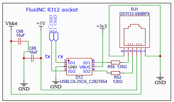
Yeah, that’s pretty much how I’d do it. If it were me, I’d add footprints for a resistor and capacitor between socket and the ESD array to create a filter in the appropriate direction (ESD array-resistor-capacitor-to-0V for TX, ESD array, capacitor-to-0V, resistor for RX). I’d also add a decoupling capacitor on both Vmot and +5V at the socket.

Don’t need to do anything other than maybe a 100R resistor and DNI the capacitor, but I’d always at least put something there.

2 Likes


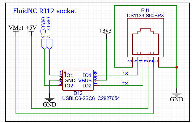
Boxed myself in real good with this schematic.

I used 120R because that is what the FluidNC guys have on their boards in case there is any tuning, we match.

1 Like

Yeah, that’s a common enough experience. These days I always start with multiple sheets and try to make each sheet a single logical sub-group, even if it ends up looking quite sparse.

120R is fine. I would add the 10uF caps with their own ports and I would always try to minimize routing from ports. They can go anywhere so shortening those lines makes it much easier to verify by eye.

I’d also add a cap to ground (even DNI’d) between D12 and R55 and then another between R52 and RJ1 so that you can make it an actual filter.

So I’d have a +5V and Vmot port on the right hand side of RJ1 with short lines. I’d add a 2nd GND port for pin 6. I’d move C68 and C69 to the right side somewhere and give them their own Vmot/GND and +5V/GND ports directly on the pin.

Me philosophy with this is that the schematic has 2 jobs. One is to correctly connect things. The other is to display clearly how things are connected to anyone looking. Drawing long traces like that doesn’t help with either of those goals when ports are involved, so they can be omitted.

2 Likes

I will take a shuffle around in the morning, thank you very much again!!!

2 Likes