When Ryan gets a board or two back, It will be interesting to see if the GPIO on the ESP-32 is blown or just those diodes.
Seems like the right thing to do.
Interesting. What model spindle was that?
When Ryan gets a board or two back, It will be interesting to see if the GPIO on the ESP-32 is blown or just those diodes.
Seems like the right thing to do.
Interesting. What model spindle was that?
It was a cheap Chineese no-name. I think it was a smalelr 500watt or 750watt one. I don’t really remember which.
I am 99% sure it is the BAT54S. I have replaced a few of them on the JP1’s. On those they would pop and the LED would stay lit.
I just checked my board, the probe clamp is connected to the ground.
Okay that confirms one of the issues, still noisy import spindles. The instructions are right, so I need to highlight that step to make it more clear.
Ah, that’s useful to know. So likely this isn’t really a new problem and it sounds like my suspicion is probably correct.
The speed controllers on those are absolute horror shows, electrically. I think in my original 500W spindle testing I’ve got some waveforms and they’re the ugliest, most basic PWM chopper waveforms I think I’ve ever seen. They’re an electrical noise firehose.
I really enjoy having a spindle, if I can ask what are the correct choices for a person that wants to run a spindle instead of a router?
What you have is great, the only downside is needing to be very careful of the probe polarity. You have no reason to switch.
Yours is significantly better than the cheapie I had. I also have a 1.5kw water cooled spindle sitting on the shelf for a future CNC build I’ll probably never get to. If yours is like mine, it has a real VFD on it, which makes it better than the crap speed controller the cheaper ones have.
You are correct sir, I am running a Huanyang VFD controlling the spindle.
The reason I asked is I am about to start my second Lowrider V4 build. This one will be a full sized unit to be able to work with full sheets of plywood building cabinetry and all for a new home we are embarking on. I really like the spindle but don’t care to volunteer for grief if I can avoid it.
Thank you for the input.
FWIW, I have one of the boards with the B driver issue. I upgraded from Jackpot 2. It did not work from the start, the Z1 motor did not move. I switched it to C and has been fine since then.
Alright guys I just took a look at the popped inputs board and it was the bat54s, swapped them both and everything works. So no ESP32 issues.
Do we know what’s popping the parts?
Well that strongly suggests static or stray charge from the routers coming down the touch plate wires if I am not mistaken.
Let’s see what the others think.
On the topic of the B/C port I have looked at it under the microscope and nothing sticks out. I am leaving for the day but will do some more testing tomorrow. I also need to double check if the multiplex chip is all the right specs, maybe I picked a weak option? 74HC4066PW,118 | Nexperia | Analog Switches, Multiplexers | JLCPCB
Realistically, it’s either over-voltage, over-current or ESD.
Over-voltage would be them getting hooked up to something above 30V which seems unlikely. Over-current would be something getting hooked up backwards, which I’d hope people would admit to.
ESD seems most likely given that the diode doesn’t have any ESD rating, is only 30V rated and is both extremely high impedance to one polarity of input leading to high voltages during a strike and extremely low impedance to the other polarity, leading to high currents.
I wouldn’t expect leakage currents from the router to be enough to do anything bad there, especially given that the router will be off during probing… Hopefully, anyway…
So yeah, ESD.
Things I’d do to solve it:
Add a TVS directly on the input.
Probably something decently sized like an SMA part if you can fit it. I usually use the Littelfuse SMAJ series but honestly that may be simply because it’s an easy part number to remember. Size the working voltage to match the input voltage or the minimum breakdown voltage to be slightly higher than the maximum input voltage. If you want to be able to handle 24V inputs, I’d use a SMAJ24 which will start conducting at 26.7V and peak at 43.0V at 10A of strike current.
Add some resistance between the TVS and the diode array.
This will limit the current in the event that a strike occurs and the let-through voltage is applied directly to the diode array. Diodes can often survive voltages above their breakdown voltage, providing the current/total energy is limited somewhat. A 1K resistor would limit any fault currents into the mA range, for instance, which is probably fine. That needs to be evaluated with the other things going on with that input.
Change the diode array out for a higher voltage one.
If the TVS can let through 43V under a big strike then choosing a 50V or 70V part might make more sense. I can’t see anything about this part that’s critical enough to warrant the slightly lower Vf of a lower Vr schottky.
Add some resistance between the input pin and the TVS/diode array.
This is a bit trickier to get exactly right because too much resistance or too small of a part and it’ll just flash over. Too little resistance and you’ve not done anything. If it’s somewhere you’ve got resistors anyway, it’s a good opportunity to move up a size/voltage rating etc. but I wouldn’t necessarily worry here.
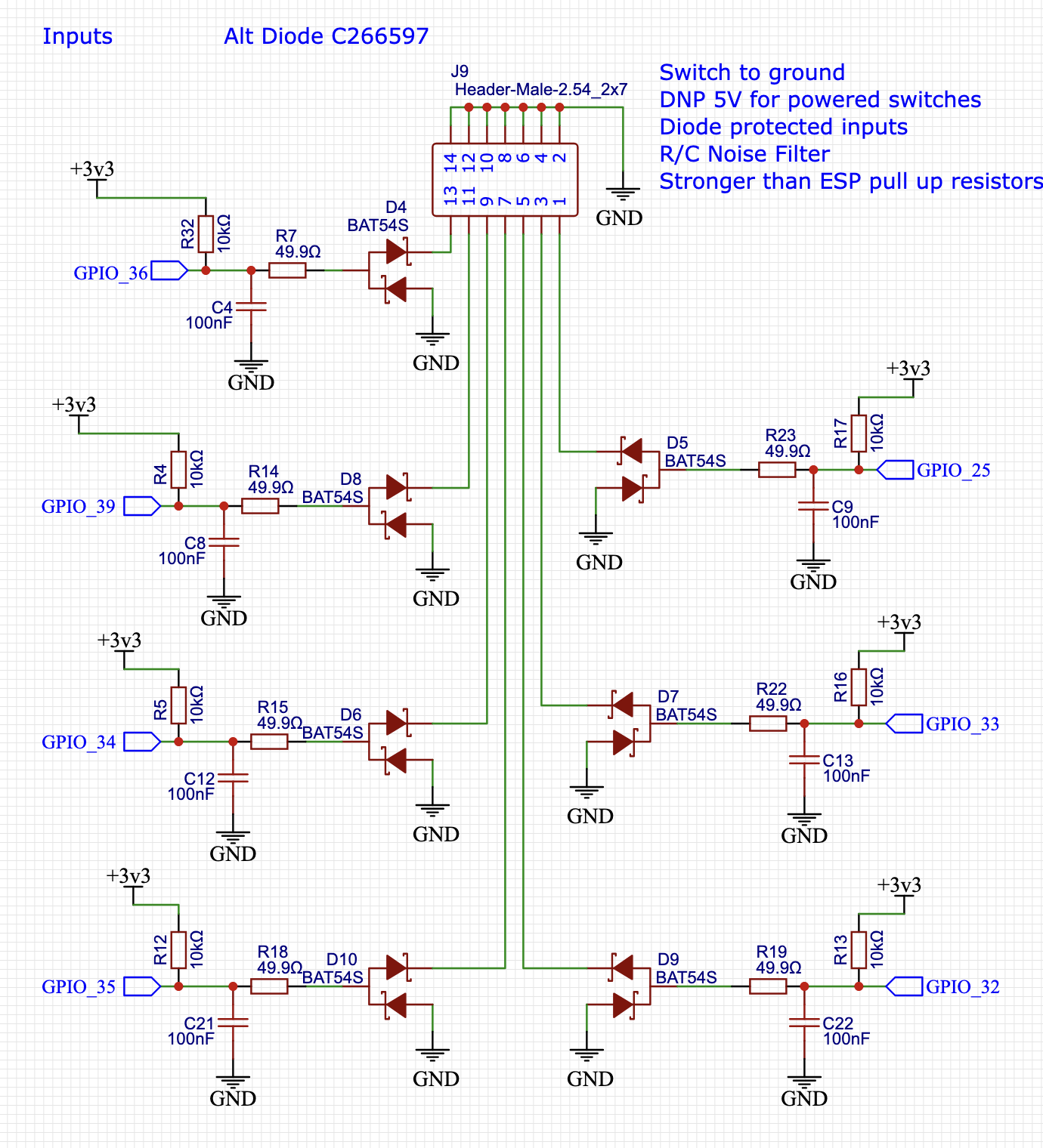
Should I just change the 49.9ohm or add it before all the stuff that is already there?
Any chance that this is the root of the issue, Would a beefier diode array solve all of this. If I am understanding this Schottky it is super fast and wastes less power, neither of these are that important to us.
Since these are just simple input to ground triggers with speed not much of a factor is there a better more simple way to handle them? Seems like this is sort of a common thing is there a 8 port chip or something with this all built in?
I kinda put them in order of importance, shoulda made that clear.
A TVS or dedicated ESD suppressor is the only real option here. Second best would be a different input device that has ESD ratings, which is a major change. Third best would be to change the inputs such that the impedance is high enough to not be bothered by ESD, which can be a challenge to verify.
Usually moving that resistor would significantly change the behaviour of that circuit, but given the slightly weird behaviour of that input with the diode array there then I don’t think it’d matter. With the input at 3.3V or above it makes no difference. With it between 3.3V and 0V it makes no difference. With the input below 0V it limits the current through the diode array which is a good thing. Resistors aren’t inherently ESD proof but they’re an order of magnitude more robust to ESD than semiconductors.
Increasing the value of that resistor also doesn’t do much that’s bad. The things to consider are the filter frequency, the pull-up value, the voltage range on the ESP32 inputs and the leakage currents. There’s also the wetting current of the contacts to consider. This is definitely something where some actual design targets and a methodical work through the design process is needed, otherwise you’re at risk of having a board that works well vs ESD but has inputs that don’t trigger reliably in some people’s setups, etc.
Eh, maybe but not really. The standard for ESD strikes defines HBM (human body model) strikes in the range from +/- 2kV up to +/- 16kV. That’s basically a 16kV charged 100pF capacitor connected to your circuit via a 1500R resistor. Given that a positive ESD strike on that pin basically puts that diode in full reverse position, it’s trying to block 16kV, which it’s not going to do, so it goes into breakdown and starts conducting. 16kV and 1500R is a peak current of a 10A, which is plenty to vaporize the bond wires or junction on such a tiny diode. If you replaced it with a much higher voltage diode it’d maybe help a little but it’s still going to go into breakdown against any kind of ESD strike. If you replaced it with a much higher current diode then it’d be less likely to be damaged during the breakdown event but that’s not something that’s a design spec so I wouldn’t advise it. It might help, it might not, and if it isn’t in the datasheet then you’re making a guess which is either completely blind, needs to be backed up with experience or needs to be rigorously tested. So completely blind, then ![]()
That’s basically it, but I always try to push newer engineers to avoid using generic terms like faster or more efficient and instead think about the actual effects in play. Once you understand the effects then those terms can be a good short-hand, but in the meantime they muddy the waters.
A schottky diode is ‘faster’ in that it has less reverse recovery time, which is the time taken for the diode to actually start behaving like a diode when it goes from conducting forward to being in reverse. Using a slow diode with a fast AC signal can end up with it not being much of a diode at all and just conducting like a really shit resistor. The reverse recovery time of a high current standard diode (like the 1N400x series) can be in the 10s to 100s of microseconds while a low current standard diode intended for small signals (1N4148) might be in the range of 10s of nanoseconds. Schottkys don’t really have reverse recovery, as such, but they do still exhibit some of that behaviour due to junction capacitance, so that might be still in the 10s of ns for a 2A higher current schottky. So here it’s not really ‘faster’ in a practical sense, so much as it’s less reverse recovery for a given current rating/application.
The other thing is ‘wastes less power’… I personally wouldn’t think about circuit performance in those terms. I can’t put my finger on exactly why I’m concerned about that sentiment, I think it’s because that’s more of a large scale overall system consideration. A better way to state that is that they have less forward voltage drop. So a schottky like an SS14 might have a 500mV drop at 1A while a standard diode like a 1N4007 might have a 1.1V drop. If your 1A power supply goes through that diode then that’s definitely worth considering, both for power dissipation/heating and for overall efficiency. One will be 500mW, the other 1.1W. In the same package size, the schottky will run cooler and save you a realistic and noticeable amount of power. In this application, if the switch is open then no current flows, so no loss. If the switch is closed then current flows from the 3.3V rail and 10K pull-up, so ~330uA. Looking at the datasheet, at 25C that’s maybe 300mV of drop at 330uA with the BAT54S and 450mV with a standard diode that’s roughly equivalent (BAV99). That’s 100uW for the BAT54S and 150uW for the BAV99. Both of those numbers are so close to zero from a component heating perspective that they’re irrelevant. There’s also no difference in actual current draw in the circuit because it’s the 10K pull-up that’s making the vastly biggest impact on the current. It’s actually a somewhat difficult thing to calculate exactly because the forward voltage of the diode changes with current through it, but you can usually get a gut feel by looking at what parts of the circuit have voltage across them. The input voltage is 3.3V. By definition, we need the ESP32 pin voltage to be 0.8V or lower to register a low logic input condition. That means the pull-up will always have at least 2.5V across it, most likely more like 3V. So it’s defining 90% of that circuit current while everything else (filter resistor, diode, connector, cables, switch etc.) are defining the last 10%.
So I definitely agree, neither of those things are important, but I think it’s valuable to understand why they’re not important and the scale of how important they are, because there are definitely times when they are.
In this case I’d say there’s zero problem with changing to a higher voltage standard diode instead of a lower voltage schottky, but I’d also say it’s not a solution to the issue, just something that makes it a little easier to engineer an actual solution. A 100V diode is not going to stop a 16kV ESD strike vs a 40V diode. However a TVS that will stop a 16kV strike might do so while letting the voltage climb to 50V… That might be enough to hurt the 40V diode but the 100V diode won’t care.
I’m sure this seems simple to you, but it’s misleading. This is actually a really tricky thing to do. You have an input that goes from high impedance to low impedance, is operating at logic level voltages but can be connected to 24V, has long lines going out to unknown conditions, made of whatever random-ass cable, installed by DIYers, connected to who-knows-what and often not even connected to anything at all, all while being intended for direct handling by (electrically) untrained operators in an uncontrolled environment with known static build-up hazards! You’re basically designing the embedded hardware equivalent of a lightning rod.
What’s ACTUALLY simple is if the circuit doesn’t leave the box and it’s kept well away from any seams/openings. Then no ESD strike.
Or it’s a long cable the goes to a permanently circuit in an enclosure at the far end. Then the ESD strike is straight to ground and is all common mode (affects all inputs the same, no damage).
Or it’s a solid molded block at the far end to insulate it high enough.
Or it’s assembled in a factory like the ones I use that have ESD dissipative flooring, dissipative tools and jigs, dissipative workstations, trained workers wearing dissipative coats and hairnets, shoes with heel straps that dissipate ESD to the ground, check-stations that workers use to verify they’re conductive, specific procedures to follow to avoid ESD damage, etc. etc. etc.
Or they just have enough space on the board and enough margin to put protection components on.
Or control the input spec well enough that it’s easy enough to protect, i.e. logic level inputs that will always be logic level, no +24V or higher, etc. No impedance shifts from on to off, etc.
Obviously some of that is straying towards hyperbole, but not that much! In anything I design for industrial/rugged applications, I’ve always considered the outside world to be deliberately hostile. When designing things for use in a sea port application, we had to consider that they’re be wired up by electricians who didn’t give a toss about the hardware. I would design everything, even logic level inputs, to survive being directly connected to 230V mains. My current designs are components to be permanently installed in equipment but that installation is still being done just in some warehouse somewhere and they need to be swappable in the field which may be a chilled/sodden meat packing plant or a metal casting plant with who knows what in the air, with the work being done by unknown technicians with unknown training/procedures etc. So I know this and design in protection at the start. Usually a TVS, always filtering, usually also a bypass diode to rail, usually a PCB layout with guard traces around the edge of the board and full coverage 0V reference planes, usually individual or multiple 0V connections for each input harness, usually provision for a shield termination, etc. etc. All of that adds size, eBOM cost and design cost, of course, but these designs have lifetime quantities in the low thousands so even a single failure makes the stats look shitty. That and when it’s going into a $100k piece of equipment, my customer isn’t going to be stoked when I explain that it failed in the field because I was trying to save them $1.50 of eBOM.
Obviously you’re in a different situation than I am. Your customer base is vastly more cost sensitive than mine and that’s what you’re trying to differentiate on. That puts you in a harder spot to design for than I’m in, which is pretty amusing if you think about it… People really, really don’t comprehend how hard it is to design well for low cost. Automotive and consumer electronics are basically miracles.
So, I can’t really help with some aspects of this. I’m always willing to spend more money on a more reliable part, so my natural tendency is ‘do it right’. I would absolutely put on a SMA TVS or ESD suppressor array. I’d probably also add common mode chokes and half a dozen more filtering components. I’d grow the board 20mm and give myself a clear 0V ring-fence and DMZ for the protection components. I’d probably isolate the inputs so that an incorrect connection doesn’t fry the entire board, etc. etc. That’s probably not the right choice here.
This is also why usually it’s best to design to a criteria… Something like ‘this input must survive 8kV HBM ESD for 10x strikes, lifetime’ . You can then try a few things and see what happens. Maybe that’s just increasing a resistor, maybe that’s adding a huge SMC TVS or MOV. Of course, figuring out what the spec needs to be in the first place is a huge job in itself, but that’s just how it goes.
Anyway, from a practical standpoint, I think the best options would be:
a) Add a note asking people to be careful about ESD, then just assume you’ll have to replace some percentage of boards. Could also suggest diode replacement for those who are capable.
b) Add the biggest TVS you can fit to that one input and make it specifically the probe input. Maybe shuffling a couple of components, too, or changing the existing diodes.
c) Make a new probe or adapter that has the protection on it. If it’s part of the probe, you’ll need to insulate the protection/connections to the probe enough to avoid it sneaking past.
d) Rework the entire input section to include ESD protection for anything that might be touched/handled while in use.
Personally I think b) or d) are the only realistic options.
No, what I mean is our use case for the inputs is simple in that we are triggering to ground and doing it once not ghz speeds.
I am not trying to offend you, I am trying to understand, and verify that I do.
My level of EE has got to be far under what you are assuming. I spend hours decoding your replies desperately trying to understand what they mean. So when I condense it to faster, or less efficient, I am trying to get confirmation that I am understanding it. I can read things like Vf and Vr, but to me that means nothing. I have to look those up and it takes a lot of time to decipher these things. So I take notes and try to put it all together in context of the situation I have gotten this board into. Then I condense it down to one sentence to express how I have come to understand something.
Well you have just experienced me moving the needle on the “must survive” to “more static that anticipated”. I thought the diode we had there already was basically bulletproof I mean we have sold thousands of these jackpots over the years and A lot of Barts boards used to use them as well. I was pretty convinced are just got a bad batch of diodes or I need to find a more reputable brand but you are making it sound like I am trying to do the impossible with protecting the exposed touch plate.
I have room on the last two inputs to add a tvs pretty easily.
This seems like the actual right way to do a touch plate. But I am sure this already exists and I can just buy them. I will start looking.