Jackpot 3 changes?

Seems we have a couple common issues here.

Inputs popping - do we switch to opto-isolation? Any other options, filter, zenier (I just guessed because that sounds cool)?

I suspect static is the culprit on all occasions. Same circuit as the JP1 and we did not have this issue as much, but I think the JP3 is selling much faster than the ! So maybe it is just a numbers’ thing.


Driver port B & maybe C. I think we have seen 3 out of 600-800 boards with a B port issue now. Any ideas what to look at besides the traces? Could this be a firmware thing, slow it down a little? I think all three work to some degree, all three test fine with $ss, but usually fail after a little use. Work again for a while after a reset. What tests do you suggest?

Do they work immediately after reset?

That sounds like the communication with the drivers is just barely stable and the B one is the least stable due to routing

If it takes some time, I’d suspect a bad solder joint that lifts of once the driver heats up enough

I think so. I am getting one shipped in now.

1 Like

Inputs:
What’s the actual description of the fault? What ports are going bad? Do you have any of them to hand to investigate further?

As I’m sure I’ve said before, without something of a diagnosis it’s hard to effectively solve a problem.

If it looks like it’s ESD then I’d expect to see the diode arrays failing open or short. I’d be adding TVSs between the connectors and the diodes.

Opto-isolating won’t necessarily protect you because the isolator can still be damaged by ESD. Filtering helps but it’s not a primary solution for that same reason. A TVS is basically just a large and inaccurate zener diode that has been created to handle excessive currents.

Drivers:
Do you have any of the boards that are failing? What do the step/dir pulses look like on the boards that are failing? It could be a soldering issues as mentioned above, it’s definitely common for issues to manifest as failing when hot or needing to heat up to start working. I’d take a careful look with a magnifier or microscope. Sometimes pressing the tip of the pin down with a scope probe or similar can make it start working, which is a good sign it’s a solder issue. Alternatively trying to gently pry each pin up with the tip of a very small screwdriver or a scalpel blade will show if it’s moving/loose or not. Definitely don’t re-solder it until you’re sure, as the single most valuable thing when diagnosing a failure is a board that reliably fails. As soon as you’ve ‘maybe’ fixed it, you no longer know.

1 Like

From what I can tell, they arrive working and fail after some use.

Usually the touchplate, I have one getting shipped in this coming week.

I have one coming in, I might have one here. I need to check. The part that gets me is I am fairly certain it is the B port that is the common issue. If it was a solder issue I would guess it to be random drivers not always B.

Or something like a deformed / misaligned pad on the B driver either in the ECAD or on a specific run of bare PWBs.

1 Like

Okay, I just checked. I have two boards here with a B/C port issue. They were from the first or second batch. I will have to see how old the one coming back is. I will put these under the microscope in a bit, but I know I have looked at them before and nothing seemed off. I will look again before the o-scope.

Touch probes going bad would certainly be plausible for ESD. They’re basically an antenna/lightning rod for most of their lives with a side of occasional machine-model ESD strike if the ground wasn’t clipped first.

Sadly I wasn’t able to snag an ESD tester from my previous job but I’ve seen diy or cheap ones for fault finding available. Bartek ESD1000 is one I’ve seen before. Not really a proper bit of test equipment but could be useful in a fault finding or diagnostic sense.

1 Like

So without an esd, and assuming this is static, could you recommend a fix?

That looks like a car battery powered hot glue gun or something.

1 Like

Well, my suggestion would be the same things we’ve discussed in the past with respect to ESD hardening the design. TVS (transient voltage suppressor) and more filtering, really. The actual fix depends somewhat on what device is actually dying due to the ESD strike, though. If it’s the diode array at the start, higher voltage diodes and a TVS will be fine. If it’s the ESP32 itself, probably a filter or another pass diode to rail as well as the TVS.

I think we went over this with the port for the pendant but didn’t bother with the inputs because there hadn’t been any issues with previous revisions. It may be a change of device, change of housing design, luck, more in the wild, all sorts of reasons why it’s cropping up now.

Not even that, the clamp is for the 0V reference and pulling the trigger strikes a piezo element and generates the ESD strike. It’s essentially a very slow, slightly shit tazer…

1 Like

The one with the JP1 I sold to Italy had the touchplate stop working from one day to the other as well, we never figured that out. :disappointed_face:

Did the user live with it, or replace a board or what?
If the board was replaced, where did it end up?

He lived with it. He just cuts his chicken coops, full through. So 0 on workpiece is fine for him as well. :stuck_out_tongue:

1 Like

Okay, for me and my limited electronics understanding, if we already use a component on the board, I have zero issues adding them in other places. If there is a minimal impact on pin performance I say, why not. If it is adding a bunch of unique things to the BOM that makes kind of a lot of work for me. I pre-oder most of the components before I order a batch of boards but still sometimes things run out or the manufacturer wants a minimum order of 20k components or something. Since I have to ask you guys if I can substitute components I want to minimize the stuff I have to depend on others for in case you are not around in the future.

I just assumed Opto-isolation was the end all be all of protection, if it isn’t lets add a few things to see if they help. Any specifics I need to look for?

What any soulless commercial brand would do is calculate how much the change would cost them over swapping three out of 600 boards (if it’s only 3). I actually think three’d be really great. There might be more where people don’t notice or are not getting back to you though.

I fought all of you guys on every penny of this JP3, like I do with every design, but something is different even though the circuits are the same, and adding a few more pennies is the next logical step. I also have no legs to stand on if doing it the minimal way is not robust enough, then more is needed.

As always throwing money at a problem is just against my soul ethos, but it has to function correctly within the bounds of the design before price is even a factor. So let’s not protects against floods and direct lightning strikes but let beef up the inputs to try and stop whatever the heck is going on.

1 Like

Let’s get some failure analysis done before you try to change anything.

It could be a production issue or even just you selling more boards. Thus seeming more of a rare issue.

I think we should start thinking about the probe and probe circuit. Having return and supply wires on long flying leads around a rich ESD environment does sound like it might be calling out for a hardened circuit though.

2 Likes

Absolutely, diagnose before “fix”. Just wanna get everyone’s brains thinking about it.

The other option is adding something to the probe.

I’d say one thing that will help you in the long run is to stop using this term ‘throwing money at the problem’.

You’ve got 3 options here. One is tons of design, testing and verification work involving probably expensive test equipment to find the cheapest solution. One is to put what may not be the cheapest solution. One is to do nothing and live with having boards come back or the e-mails from people asking for help.

It’s not about the cheapest board or the lowest eBOM or the fewest parts count. It’s about overall price vs performance. No sense in saving yourself 10c/board and spending an hour e-mailing every 50th person who happened to go full Palpatine on the board because they were wearing polyester underwear while they were using their CNC or whatever. How much per-board is worth not sending out replacements? Etc. etc. etc.

Anyway, on a less preachy note.

Definitely wait to see what is actually dead and how bad it is. That’ll give a rough idea of next steps. Under the assumption that it is ESD on the probe and not something else, I suspect you’d see dead diode arrays on the input (either completely open circuit or short circuit) and/or a dead/unresponsive micro input.

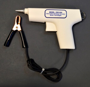
My personal approach would be that if the probe circuit is dying to ESD then all the inputs probably need beefing up, but that’s likely overly conservative for what you’re after. If it is just the probe then are you ok with having a separate header for the probe or a specific input that the probe must be on? If so then we can add ESD protection to that one specifically.

Adding something to the probe could work. ESD straps build a 1MR resistor into the line to limit peak currents to prevent ESD damage. Adding that to the probe could work, but you’d want the ‘unprotected’ side insulated enough that it couldn’t take a direct strike. Alternatively you could have the probe connected through an adapter board that had some form of ESD protection and added impedance to both sides of the circuit.

Ideally, you’d probably want the earth strap for the probe to either be permanently connected to the router or to have its own limiting , under the assumption that a potential source of ESD is connecting the ground clip. That may be mitigatable by ensuring that the circuit itself has at least some impedance to the installation earth, even if it’s high impedance.

My logic here is that you’ve got 2 open connections to your circuit that are being handled by a charged human and then being connected to something that could be charged or that your circuit may be getting charged via the long lines running everywhere and then be discharging into an earthed/uncharged person or machine. ESD strikes via people tend to be higher voltage but less damaging. ESD strikes via machines/other circuits tend to be lower voltages but higher energy so can be more damaging. An ESD strike into the ground clip won’t be as likely to hurt things, but it could still cause damage. It will depend on how the rest of the circuit is wired, whether the power supply 0V is earthed, what the inductances/impedances everywhere are, what the impedances to other connections are, etc. A big pulse of current down the ground strap and out to installation earth can cause the 0V reference (GND) on the Jackpot to change voltage briefly vs other things its connected to which may be enough to hurt stuff. An ESD strike into the probe itself will take one of two forms depending on polarity. It will either be a high-impedance strike to the diode array which will cause a high voltage to appear on the input, potentially tracking to other adjacent inputs, or it’ll be a low-impedance strike through the diode array, potentially damaging it. All of those situations can also occur as no damage, partial damage or catastrophic damage, depending on the scale of the strike. Even repeated small strikes may cause long term drift in specifications at best or outright damage at worst.

3 Likes