Oh, and do we have a component on the board already? I remember discussing one but I’m looking at the linked source in the docs for the Jackpot3 and can’t see anything. Is the one listed in the docs the latest?
Yeah this one is the latest as far as I know, Invite - EasyEDA - Online PCB design & circuit simulator
Ah, never mind, it was right in front me me the whole time. I was looking for something like I’d draw it, which is usually with the zener and diode array called out specifically.
Right, so that should be fine for any of the inputs but it will limit them to +3V3. If you’re ok with the inputs needing to be 3V3 logic level or connected to open-drain drivers then you could replace the schottky arrays (D4-D10) with those instead.
You could also bump the filtering up a bit further if you wanted. 50R/100n is ~30kHz corner frequency so ~10us step response. Pushing that to 4K7/100n would give you ~3kHz corner frequency and 100us step response, or even further. That’ll only do anything if you’re seeing dead micro inputs, though.
If you’re seeing dead diodes and want to keep those inputs as capable of +24V or whatever then your only option is something like a 24V TVS, which would be a new part.
 Now now, you know I do it differently. I squeeze it in where it looks cool in the schematic because I have very little fundamental concept of what it is actually doing. Form before function, I am pretty sure that is how everything is supposed to be done.
No, that was absolutely my mistake. It’s in the correct place, I meant the component itself, which isn’t something you drew.
I like to try avoid ‘square box’ type components for things that can be represented as discretes. So things like an optoisolator will look like an LED and a transistor inside the box. The box as an outline shows that it’s a single integrated component while the components drawn out make it a bit more obvious at first glance what they are.
This enhances readability of the schematic in that you can tell a devices function and check for correct connections without needing familiarity with the component or to open the datasheet etc.
That’s how I learned them 
That’s more an issue with EasyEDA though than Ryan’s schematic proper.
Well aware. I’m explaining why I didn’t see it.
Edit: In a way that hopefully adds some context as to why I think Easy EDA is still a ‘not quite there’ tool, in a bunch of ways.
Don’t know if this will be helpful, I hope so.
My probe was not working after I changed out the core a while back. I lived with it for quite a while before I decided to dive it and find the issue. What I discovered is when I would touch the spindle with the ground it would trigger the probe light on the board. I have no idea why or how this could happen. I traded the wires around and all is good. I did not destroy the probe function just the had the polarity reversed. It is working wonderfully now.
It should be wired ground to spindle, is that how you have it now? Or am I getting that part wrong? Also what are you using a spindle?
AS
As far as I know it is wired per the instructions.
This is the spindle I am using along with Bart Drings Isolated RS485 CNC I/O Module***.***
This is the setup I have been using for over a year with no issues. I reprinted my core in PET-CF, when I did the change out the probe failed. Once I reversed the probe wires all has been working perfectly.
I am running a Jackpot V1, I hope I didn’t waste your time sir!
Never, you just gave another good data point.
Those spindles are notoriously electrically noisy and have caused all sorts of issues like this. If you get a chance next time you are out using it see how it is wired, the clamp should be on the ground pin, if that is not what worked for you I need to look into this one further.
FYI
I did purchase this cord for running power to the spindle. Checkbook got grumpy but I have never had an issue using the spindle.
16AWG 1.5mm² Shielded Chain CNC Wire (12FT) UL2464 Tinned Copper Core Extreme Flexible 16 Gauge 4 Core Cable Electrical Wire for CNC Router Machine, CNC Spindle, Robot Arm,3D Printer,etc
Should I wrap a wire around the spindle and tie it into the grounding for the vacuum system? I have never done anything other than hook it up and hit send.
I will check and confirm the clamp is connected to the ground next time I can get in the shop.
I don’t think it is a wiring issue, I think those spindles do something weird with the ground or have some stray current or something. Not all of them but it seems like a 50/50 split.
Looks like I got lucky, I will take that win!
Looks like I got lucky, I will take that win!
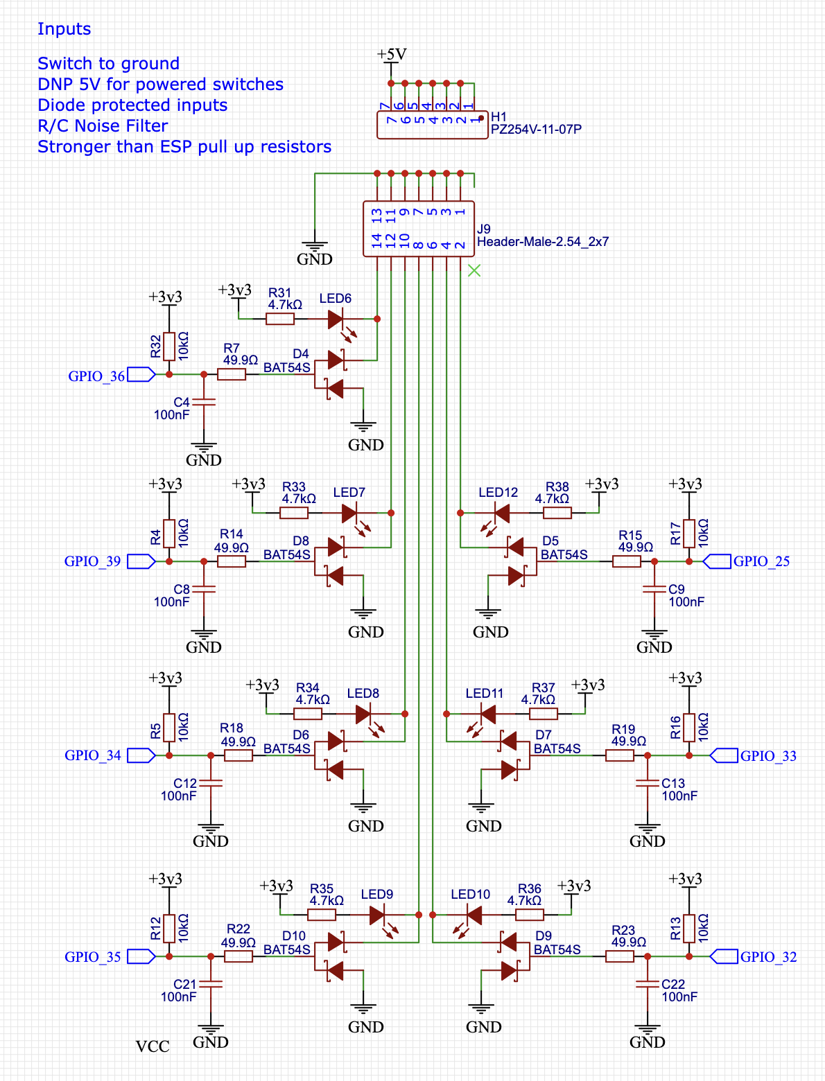
I just did a quick refresher look at Jackpot V1 and V3 comparing the inputs.
This after another forum thread about a V1 user that went to V3 and promptly blew the inputs.
The only difference I see is removing the LEDs. I’m not sure how the LEDs would provide any robustness improvements, but I’m thinking about it.
Jackpot V1:
Jackpot V3:
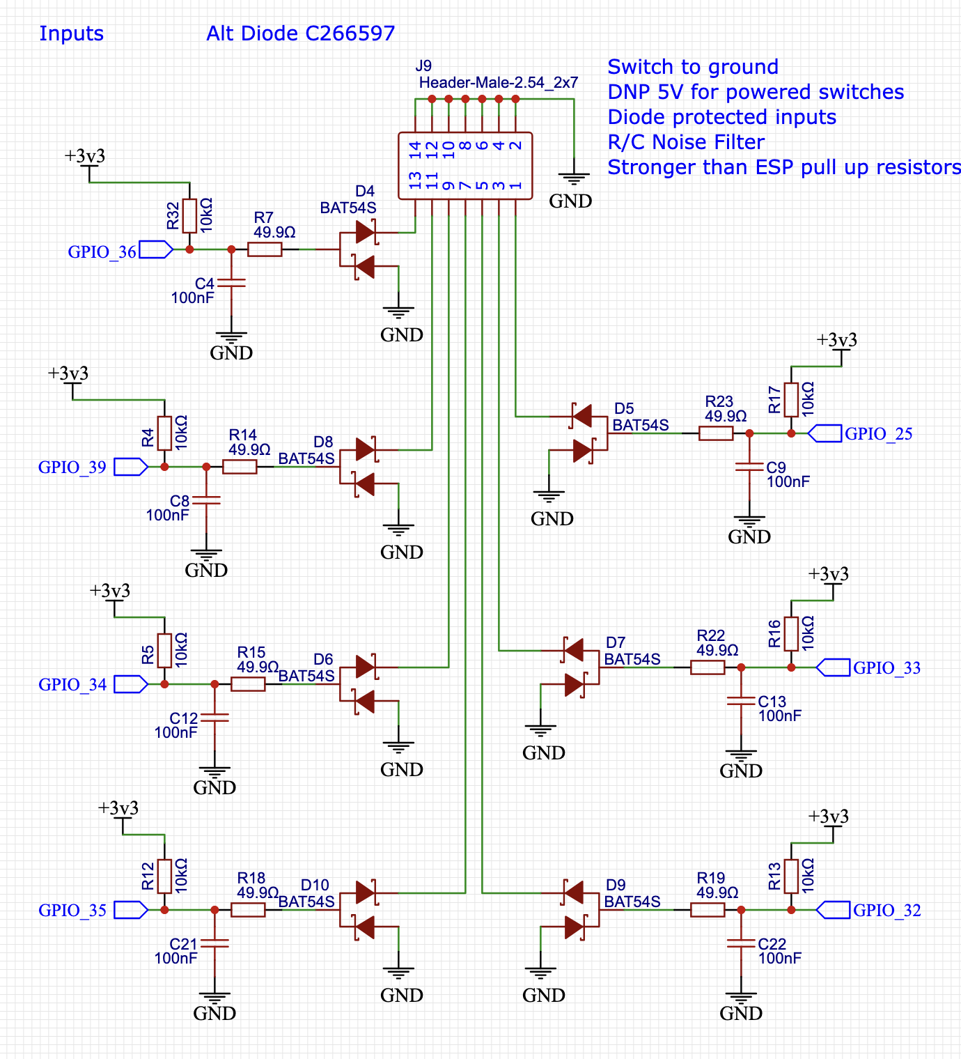
The schottky array at the input limits negative voltages to roughly 0.7V, is that already enough to damage the esp? That would be further reduced by the voltage divider on the input as well, but it’s to early for me to do math.
The LED would act as an additional pull-up, reducing negative voltage spikes from esd events.
The problem with voltage limits on micro inputs is they’re not really a voltage limit so much as a blocking voltage spec before any current will flow, then there’s an unknown amount of current that can damage a pin. The ESP32-WROOM-32 electrical spec is -0.3V, but it’ll usually take more than a few mA to do any actual damage.
Assuming 10mA into the input, that’s 0.5V across the 50R resistor so 0.8V needed across the BAT54S. That’s ~200mA into the pin and through the BAT54S until it’s at 0.8V. That’s at DC, though, so the actual waveform of the ESD strike needs to be considered due to the RC filter, there. The frequency components of the strike are well into the GHz range, though, so the impedance of that 100nF cap at ~1GHz is also not likely to be actually 100nF… The diode will also have some capacitance across the junction which may be enough to be important in the GHz range. Tough to tell, but I would be more worried about the diode array itself being damaged during an ESD strike than the micro pin, personally.
I would assume that the LED will have absolutely no effect at ESD currents from a pull-up perspective as it’s directly connected to where the strike is occurring. The current through the LED is negligible for this situation and even if it went full 0R breakdown in reverse, there’s still a 4K7 resistor there. It could also be that a newer silicon revision or different model of ESP32 is being used here, or that there’s just less inductance around with the ESP32 soldered directly to the board…
Regardless, adding a few chunky TVSs would be my approach and then reducing the corner frequency of that filter significantly.
Hmm, could one add those on the wire side of the connector, just to be sure?
Yeah, that’d be my approach. I usually try to design the board with as close to an uninterrupted 0V plane as possible and then I’ll put a 0V guard trace around the perimeter of the board on all the layers with vias stitching them every few mm. Any ESD protection can sit outside the guard trace and has the signal routed with low inductance through the pad of the ESD device. Then through some form of filter, even if the components aren’t fitted. For particularly nasty environments or sensitive devices I’d use some kind of buffer between the input and the micro.
Something like a SOD-123 TVS may be all that’s needed, in most cases, especially if there’s some filtering/clamping downstream to handle the voltage let-through of a smaller TVS.
I had written a pretty large reply that basically boils down to this statement.
I had a smaller spindle that had the same issue. You could almost feel the static coming off of it when it ran. I had to add an earth ground to the case of the spindle to fix the issue.