I know some of you have a ton of PCB design skills.
I am eagerly learning easyeda, and it is pretty fun. I am missing some CAD like features but I am getting the hang of it.
First question is trace width. - Specifically the drivers power pads. The 2209 has a peak amp draw of 2.8A and an RMS of 2A. I know we will never really hit either of those numbers but why not design a board capable of it. So do we design to RMS at a minimum, and assume any peak draw only adds heat momentarily above the 10C max rise specified? IS that why the large caps are there to handle the peak spikes?
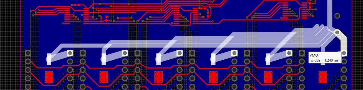
Step one - keep the power as close as possible for short traces. We have 6 drivers, max of 85mm or so away. The calcs say each trace needs to be 1.24mm wide individually.
If I add up 5 of them, since all that current will need to pass through at one point the calc says 11.4mm wide. That is not 1.24*5. (RMS calcs out to 8.4mm wide)
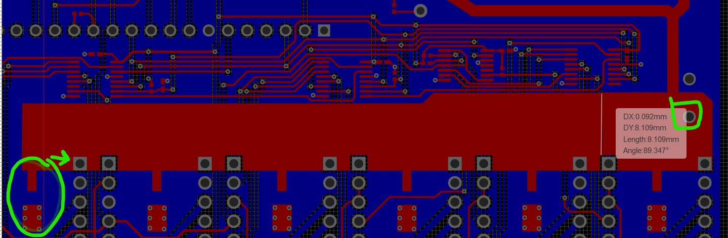
Now all that power is coming into a single plane at one through hole. How do the electrons flow, as in what shape should the copper area be for ideal amp flow? Straight line, how far behind the through hole should it go?
The big green circle is the large cap, charge bank?. The green arrow is the actual driver in. Green square is the power in. So you can see I am not too worried about driver number one right under it…and that one can actually have power on both sides of the PCB.
In my head, this is what I imagine a more efficient use of space looks like. Obviously in one large pad, I just used traces to illustrate my thinking. Why is this wrong? I am also a little curious about that small leg to the driver in from the cap. Is it better to go straight from the cap, or right to the copper area, electrons are electrons, right?
This works 99.9% of the time, including this case where you have inductive spikes from the motor that will be too short and infrequent to appreciably add to trace heating.
Yes the caps are there to feed instant electrons to deal with transients that the “upstream” traces and supply cannot deliver. This is why it’s important to have the cap positioned closest to the source of the spikes (ie, near the drivers). The further the cap is from the items that will use it, the more resistance those electrons will run in to going from point a (cap) to b (load).
Generally speaking until you get into very high frequency signals (think modern PC RAM or rf feedlines), you don’t really have to worry much about the shape of your traces. For DC supply lines, the trace should be good to go as long as the minimum trace width is satisfied (RMS) along it’s length. In other words, that trace for the driver on the right side is fine IMHO.
[edited: NM… saw your supply is coming in from the green rectangle on the right. That’s fine, but the cap should also be on the right side… not the left for best performance. Think of it like this… if the cap is on the right, a transient comes along and quickly discharges the cap, now current has to flow across all those traces to refill the cap. This is not ideal as the current to and from the cap will result in more voltage fluctuations across the traces. Keeping the cap immediately “upstream” allows it to deliver electrons properly across the tapered traces, and it gets recharged directly from a lower resistance connection to Vm.]
So this style is ideal, meaning the cap pad and power in pins are all connected, and the trace width can step down at each capacitor pad.
That actually frees up a lot of room shifting all the chips above over and down.
I have also learned to not design to the manufacture’s minimums. Also leave as much room between traces as possible, should not matter much here but I was grouping traces close, and that is not best practice.
This stuff is fascinating and I am learning so much. There are so many ways to route and place items. Super interesting. I am just cloning someone elses work and messing around but I am sure at some point I will run some of my own boards.
Yeah PCB design can be really fun; I liken it to solving a jigsaw puzzle. I often find it beneficial to step away from a jigsaw puzzle often, to let me mind reset etc. The same idea works with PCB design (heck, any engineering design really)… it’s a good idea to take breaks often and allow time for new ideas may come to surface. That avoids the dreaded situation of ordering PCB’s, then a week later discovering that super neat idea that changes everything.
What you can/can’t get away with as far as design limits will of course depend where you get them made. It is a good idea to design things to be easier to manufacture, as that will open up the options for board houses that can handle it (ie, lower pricing). Also even if your design fits “min specs” for a manufacturer, they will account for challenges WRT the processes they use as they relate to your design. So if you pack a ton of vias and traces, have sketchy thermals (tombstone risk, etc), and likely other items I’m not thinking of… they will calculate the higher risk of failure, and you will end up getting a higher quote as a result. This is why it’s nice to have a good contact at a board house that can articulate these kind of issues to you as you get closer to having them made.
It is hard to be creative when you are putting a lot of pressure on yourself. I was onsite for a week doing some intense work and I came up with our best ideas while I was driving to dinner. Creativity just can’t be forced.
That is crazy. I get amazing ideas while I am driving. I assume it is one of the few times my hands are busy but my mind is in cruise control with the task at hand.
I have said for a long time that one benefit of working from home is you can shower in the middle of the day, which helps creativity. Most people don’t want to think about it, but it really does help.
I ride the same bike lane everyday. 10 km each way, all year round. Today I passed 11 111km on my second ebike. Very apparent thoughts pop up in my mind on the first tall bridge. Deeper and more complicated ideas/understandings occurs on the last hill reaching work. It’s fascinating how the physical activity and movement through the landscape facilities mental processes, without actually trying to!
Still ~80x100mm, using 2 or 4 layers? 4 layers cost more (e.g. FR-4 Black 100qty, 2 layer ~$0.47 per board, 4 layer ~$0.95), but only slightly more when full board parts/assembly is considered. Would routing proper Grounding/Power and signal return-paths/shielding for signaling be easier with 4 layers, minimizing interference, with a good layer stack up ?
Curious what PCB designers here recommend? Would be nice to see this board be useful for various scenarios, but am not expecting to be used for everything. e.g. Someone working on mostly printed electrogravitic propulsion build may want to consider an alternative more heavily shielded board design.
Coming from a guy who graduated in comp sci + AI + electrical eng ~25yrs ago,
watched a bunch of PCB related YouTube videos, and has only made 3 fabricated PCB designs, and one of which was a Pioneer Sat plaque inspired beer coaster…
Am most creative when taking a drive, stroll, jog, poop, shower - Basically any time and space where mildly physically occupied, but cognitive bandwidth is free to wander uninterrupted towards an idea, or beyond a local maxima we’ve overly tunneled visioned into.
No, Currently it is now 90x100. Yeah taking a quick look it goes from $0.80/per PCB to $1.61/per PCB
Currently, 2, but I am considering 4 just to reduce the size (and to design a 4 layer board!). Especially now that you pointed out the cost difference.
I just feel like this board can be smaller. I keep playing with things and there are ways. Maybe when it tests complete, we can all give it a shot before I run another batch.
For an extra $0.80/per board, reducing the footprint would be worth it, just for the fact that the LR3 runs with the board on its back. A tiny board could be put anywhere, including in the beam, for the ultimate clean build.
I was shown the firmware does currently seem to be fully functional with the upgrade, we will not know for certain until it can be tested on actual hardware. It looks to be a green light to use 2209’s now reducing the driver cost by HALF, and increasing total current capacity (even though we do not need it). How cool is that, custom board, and custom firmware. That firmware will certainly open the door for other boards to do the same. Using the ESP32 limited IO in creative ways is Bart’s superpower it seems.
I forgot to mention… Thinking ahead to the type of compact enclosure(s) you’d want this to be housed in, and how the wiring would be run, and strain reliefed… With more layers, would moving power/signaling connectors onto the same side might be easier? Am assuming you’re going for a compact, clean, neat, wiring/housing setup?
The in and out are all on one side, steppers are on the other. Power in and the module face the 3rd side. Side 4 has the SD card slot hanging off the edge . That means one side can be close to the edge of the box and the three other need minimal space. (Some of the modules take more room than others but I think those will rarely be used).
I’d definitely recommend moving to 4 layers. There really aren’t any downsides these days, aside from a very marginal cost increase that can sometimes be entirely offset by shrinking the board.
The EMI performance increase is pretty noteworthy, especially at higher frequencies. It also dramatically reduces routing complexity because you’re not worrying about power distribution in amongst your routing layers, which also improves signal integrity etc.
A recent design was 4 layers @ 6oz, ~1kVdc, 200Arms for a liquid cooled inverter.
Other general thoughts: I absolutely design to manufacturer’s minimums, but I try to do so sparingly. If you’re using a process that will go down to 0.1mm then use that where needed and try keep it to 0.15 to 0.2mm for things like polygons/planes where there are huge lengths at that separation. If you’re using 4 layers you won’t need planes, so that’ll be easier.
Identify the process specifications you’ll be using first and try stick with those settings. Changing the design part way through because going to 2oz copper means you’re no longer meeting minimum clearances is a huge time sink.
Be very careful of the footprints for your devices. Make sure they’re close to the manufacturer’s recommendation and consider asking the contract assembler to double-check them for you. Our usual contract assembler prefers smaller paste apertures/less paste than manufacturer spec. For passives this doesn’t matter. For ICs with a power pad on the bottom, especially QFNs, that can be pretty important.
When you’re at a place you’re happy with, I’d be happy to put some time aside to run through a design review with you, similar to how we’d do it at work.