Jackpot3

I feel like I’ve been beating that drum for quite a while, so it’s pretty pleasing to see that be considered! They’re definitely not a perfect solution but they’re my favourite out of everything I’ve used by a huge margin. Typically the issues with them are that they’re much larger and more expensive than a crimped solution. They’re also missing a couple of nice-to-haves like built-in strain relief options. I’d say that for volume production they would be less reliable than a crimped cable assembly but for DIY with cheap tools and crimp inserts I think they’d be much better.

I forgot, you can even get some really weird stuff like these:


Pluggable screw terminal header in a bulkhead mountable form, QC tabs behind it. In the past I’ve just made my own by either making a backing PCB or super-gluing a line header into a filed hole.

Yeah, that’s definitely a skill you’ll develop with time. To start with it helps to try lay out the schematic the way the PCB will be laid out. To get the best out of both or as they get more complicated then there really needs to be a bit of a clean break between the two. That might mean you need another way to note things down so it’s clear which nets need to be wider traces, which have high edge rates and need to be routed more carefully to avoid crosstalk, which are sensitive inputs and need to be kept away from high edge rate nets, etc. The more ‘professional’ packages let you define characteristics on the schematic that control stuff like that on the PCB layout but it often adds a layer of complexity that can get irritating in practice. Usually my approach is notes on the PCB or a list of things as I’m designing it that I’ll go through and check off as a sort of ‘pre-review’, before reviewing the layout with a wider group of people etc.

2 Likes

Just having a play with the schematic now. I was going to PM this but might be nice to chuck this stuff out in the open so people can follow along if they like.

Extra unexpected connections:
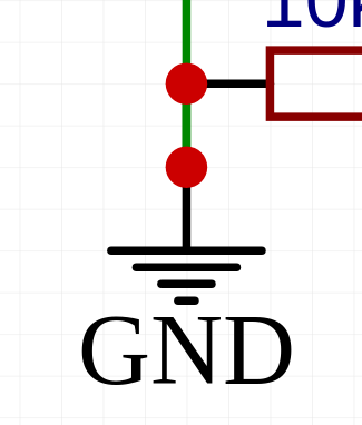
One thing to look out for is when you see things like this:


The red circle means it’s an intersection between at least 3 wires/nodes. Given that there’s only a wire and the power port there, that means there’s a 2nd wire sitting on top of the other wire. It’s usually not an issue, but I find it helps to spot that and fix it as soon as it happens, rather than have it make a mess when you drag something and it splits it into a bunch of different wires.

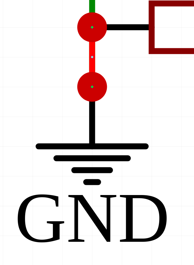
In this case, it’s just a stub between the resistor pin and the power port:


And deleting it brings it back to what you’d expect, which is red junction indicator on the resistor pin because it’s going to 2 wires, no junction on the power port because it’s just wire to port.

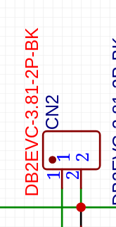
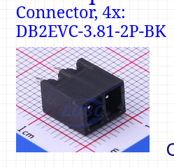
Long part numbers/connector info:


With excessively long part numbers like that I’ll often hide them and then do something like put a note/photo of the part next to them. If you need the exact part number, the BOM is where that should be taken from. If you need the rough part for review, a photo is often a better option than a part number, etc.

Dropping a note like that somewhere nearby makes life a bit easier.

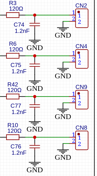
Repeated schematic snippets:
When you’ve got repeating parts of a schematic that are the same or similar, I like trying to lay them out the same and have them near one another. That way it’s super easy at a glance to see that they’re all the same or spot any differences.

Wiring between power ports:
As above, I also prefer to just use multiple power ports/GND symbols rather than wiring between them. If you want to move the connector, it just goes with it. You don’t really need to know that pin 2 of the connector is connected to the bottom pin on that capacitor, it’s not specifically useful information beyond knowing that they’re both at 0V for their function.

Designator/value location:
Don’t worry about moving the designator and value text if it makes the schematic cleaner. As long as it’s clear which component it’s for and the designator and value are together then it’s usually fine. Conversely, if they don’t need to be moved, keeping them in the same kind of location for the same type/orientation of components makes life easier. IC part numbers and designators above the IC. 2-pin passives (resistors, inductors, capacitors) that are horizontal having the text above or that are vertical having the text to the right, etc.

Schematic flow:
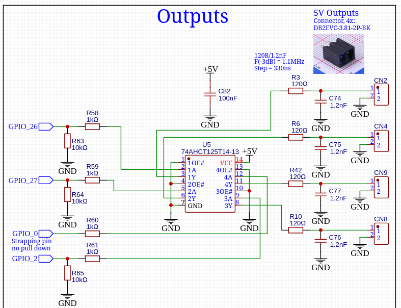
I generally try to keep everything flowing left to right for ‘signal’ flow and top to bottom for ‘power’ flow. A lot of this is personal preference, but that personal preference is informed by having spent a lot of time looking at other people’s schematics and having an innate sense of what is most common and ‘preferred’, admittedly with a very western/european perspective. That’s not a hard and fast rule so sometimes a clean schematic that flows in an unexpected direction is better than forcing the flow to be ‘correct’ at the expense of readability, but the goal should be to try keep it clean AND flowing as expected.


In this case I’ve also kept it so that the top GPIO connection flows through to the top output connector. I’d still usually put a note at the connector symbol confirming what it’s purpose is or what GPIO is driving it, etc.

General schematic hygiene:
Don’t be afraid to move components and change the schematic layout to give more space for things or to make text info easier to read or more obvious. The whole point of the schematic is to provide an easy visual representation of how the circuit is configured so that the layout is easier to get right. Having all the connections be correct is the main thing, of course, but the secondary aspect of that is having it be easy to read so that it’s easy to visually verify that the connections are correct. A technically correct but ‘ugly’ or confusing schematic is fine, it’s just a lot more mental effort to verify that it’s technically correct and has higher likelihood of not being correct as a result.

Also don’t be afraid to split into multiple sheets, especially when you’ve already got a really nice functional block layout like you’re using. Having a sheet that’s just ‘IO’ and has the inputs/outputs on it is a great way to do it, for instance. Multiple sheets can be slightly harder to work with, but the benefit of having more space to lay things out clearly and cleanly can offset that and then some. When crossing sheets I would try to make the net or port naming as clear as possible to avoid needing to refer to multiple sheets at the same time. I would also try to keep as much of the circuit as I can on one single sheet. As an example, with the IO blocks I would try to make sure that the IO sheet has everything that GPIO_26 is driving and all the components it’s connected to. The sheet that has the microcontroller on it would then just have the micro with the GPIO_26 port/net label and nothing else. There are some exceptions to that such as when parts connected to the same part of the circuit have wildly different purposes. Bootstrap resistors are one example, I’d usually put those with the microcontroller so that they’re readily visible when reviewing the schematic to make sure that the microcontroller is wired up correctly. I might put a note on the IO schematic saying ‘pulldown on other sheet’ or similar. On the other hand if all they’re doing is acting as a pull-down to make sure the output stays off while the microcontroller boots then I’d put that on the IO sheet and, if it’s important for the microcontroller review, add a note near the microcontroller saying that the pin is pulled-down on another sheet. Again, no absolute right or wrong but thinking about it from ‘what makes the most sense when reviewing the schematic to make sure it’s wired up correctly’ is generally a good start.

Other notes:
Every IC should have a 100nF capacitor placed close to its Vcc pin if just using a ground plane or nearby if using a ground and +V plane. I always put that 100nF capacitor next to the IC on the schematic which ensures that it doesn’t get forgotten. Technically it doesn’t need to be that exact capacitor for that exact IC but it’s good practice to get the details like that right. If it doesn’t end up mattering, it’s just a couple seconds extra time that was taken. If it does end up mattering it might save a few minutes of confusion or worse.


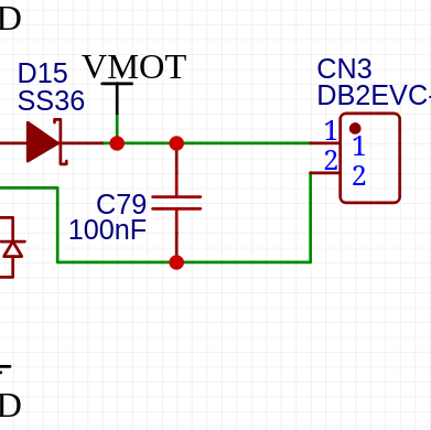
I think I might have confused you a bit here. When we add decoupling capacitors, we do that so that any inrush current or high pulses of current that occur can be supplied by a capacitor as near to the load as possible. That saves the current coming from a different part of the circuit potentially causing a voltage drop elsewhere or letting that ‘noise’ that’s generated interact with other parts of the circuit.
In this case, the capacitor is added such that it’s across the load and will supply the any current pulses while the circuit is operating, but it’s also being switched by the FET so that when you first turn on the load it will also have to be charged by the FET. Because of that it won’t help with any inrush current (such as if the load has its own capacitors on its input) and will in fact lead to more inrush because you’ve got another capacitor to charge.


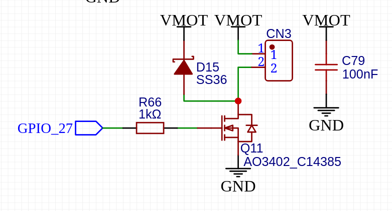
This is how I would lay that out. The logic for the current flow is that when the output is off there’s no current flow out of the connector. When the output turns on, there may be a pulse of current out as the capacitors in the load charge, for example if it’s controlling a SMPS, motor controller etc. So a brief burst of high current has to come from somewhere. Having C79 there means this current pulse will flow out of the ‘top’ pin of C79, into pin 1 of CN3, through the load, back through pin 2 of CN3, through the drain of Q11, out the source of Q11 and then finally back into the bottom pin of C79. If you don’t have that capacitor there, the current still has to come from somewhere, but that somewhere might not be anywhere near CN3/Q11 and it can be difficult to predict where and what the effect might be on other parts of the circuit.

4 Likes

That makes sense, a lot of sense.

2 Likes

Did you see the new support for esp32-s3 over on discord? Will that be v5?

1 Like

6 Likes

I wanna see you make one like this! Just one! https://www.instagram.com/reel/DK9zWcqTKjQ/?igsh=MWR6c3pzMTF6c25hMQ==

2 Likes

If I wanted to do one like this, how large would the board be? I realize there is probably multiple levels to your board, so the self cut board would probably be good sized, but would it be a computer motherboard size?

The largest issue is we use a 4 layer board, with jumper vias and a power plane. The power plane has multiple regions. So if you did a two sided board with the signal layer on one side and the power plane on the other, you could hand jump vias since there are only 10 or so. At that point you would just need to handle some manual (100 or so?) vias to the power plane. So in theory it could be the same size.

You would miss out on a lot of the surface, inner and bottom grounding planes but I assume our stuff is not fast or sensitive enough to need it, Jono would have to weigh in on that.

1 Like

Ok!, bummer! I already get alot of, “you made thats” for the cnc, but man if I could say “it cut and I made the board too!”. That would be insane!

1 Like

Ryan’s source code is open source. It would not be less expensive, nor easier, to make your own board- but you absolutely could lay out your own board and make it with a CNC.

I’ve helped kids at the local makerspace create their own boards, one key with a CNC is to have a really good way to map your bare board as fractions of a mm matter for routing your circuit board. bCNC has a good facility for this.

You’d want to make some practice boards first to get the hang of it.

I’d suggest something like a Jackpot V1 would be a better starting point as there are more socketed / through hole components there which would simplify things for you.

If you really, really wanted to do this, you could- and I bet you could get some help here for that.

4 Likes

For sure. Just last week I considered just making a prototype output section to test….on the CNC because I am not trying to breadboard the 0402 stuff.

Then there is the cost of the components, some of the stuff is hard to buy 1-2 at a time. I just had to buy 5k resistors, the price was only like $5 or something but they are not trying to sell you a $0.0001 resistor 5-10 at a time.

There are a few problems with something this “complex” There is definitely going to be two sides, and VIAs by hand suck to do. Things have to be spaced further apart, I have traces at 0.254mm gap. That would have to be larger, for sure. Stephen Hawes has a video coming for some Raw PCB making things not 100% for CNC but his new project should make PCB prototypes by CNC a lot more useful.

Sections of the board 1000% would be fun to do, just not the entire thing. Now, if you want to make a PCB…..make a module! The rj11 module for the Jackpot 1 would be super easy and fun. You can also make some indicator LED’s into a module and CNC that as well. That would be a great idea for a project. I could even get the components in bulk for cool little project kit or something.

4 Likes

You’re right, nothing here is fast or sensitive enough to need that, it’s just shrinking the design and making it more reliable in the face of noise etc. All things that wouldn’t be an issue for a DIY attempt.

With milling PCBs one of the main issues is that you end up having to use large traces with large clearance routes between them unless your setup is absolutely dialed. Really rigid and accurate setups can use end-mills for the tiny clearances but most that I’ve seen use shallow angle V-bits which means extreme sensitivity to Z. The PCB mill I had used a floating pressure foot to accurately set the height between the top surface of the PCB and the milling head, which would be a neat thing to build but isn’t necessarily an easy task by itself.

For some components those large traces and ‘spaces’ (the clearance routes) mean you can’t use some modern components where the leads are too close together etc. but that’s not likely too much of an issue for designs like this where there aren’t a ton of ultra-modern components in use, or where you can use things like the stepper driver modules to get it done.

Another issue is that single sided with a ground plane is relatively straightforward, double sided is a bit more difficult due to alignment/skew etc. Multilayer is exponentially more difficult etc.

So if you wanted it to be something easily accessible without doing a ton of work on machine setup and verification, a single sided board with a ground plane would be the best bet. Then you’d want to do it with the biggest passive components you can to simplify that single sided routing, as well as making liberal use of jumper wires. This is how we give ourselves a kind of ‘3rd layer’ by being able to route signals under resistors/capacitors etc. There’s nothing about the design that needs SMT components, so through-hole passives/ICs could easily be used where possible which adds a lot more routing space at the expense of design size.

Basically, all of the issues are layout complexity related at the end of the day. Flexibility can be your friend here. An ESP32 driving something like connectors or LEDs where it doesn’t matter which GPIO it’s connected to, a single voltage rail, maybe a module or 2 in a socket would be super easy. Trying to use all the outputs of an ESP32 effectively would get much more difficult because you now have pins you have to use for specific purposes. Trying to make a faithful recreation of the jackpot would get difficult because you’re trying to route +24V, 5V and +3.3V around, as well as dealing with enough circuit complexity that you’ll need a lot of vias, jumpers, etc.

But, as Jim says, it’s all very possible. It would best be a case of starting small and working up. Something like a PCB to clean up the wiring for a pendant would be a great use case. That’d get you a sense of how things can be routed, what part scale is needed.

Personally, I don’t really see the appeal. From a teaching kids about the processes or learning things yourself perspective I can definitely see the logic there, but I think picking an easily achievable target is a better goal. If you’re going to teach someone hand cut joinery, start with a box joint not dovetails. I guess for me I’ve kinda done my time trying to use my DIY skills to make something I can just buy. I’ve got hundreds of project ideas that range from ‘recreate something that I don’t want to buy’ through to ‘make something entirely new that solves a problem I have’ and anything in between. If it’s just to say I can do that, I’ll do it with something smaller and then move on because I know I’ll lose interest. If it’s something I want to customise slightly, I’ll try to do that instead. If it’s something where it literally doesn’t exist or has a price tag that justifies spending tens to hundreds of hours on something then I’ll definitely make that.

PCBs are cheap. Even the cheapest PCBs are, unfortunately, unfathomably better than anything you’ll ever be able to hand make. PCBs are also a component, not the ‘thing’ itself. It’s enough work making the ‘thing’. If the goal is to make the PCB then that’s great, go for it! If the goal is to make the ‘thing’ then buy the PCB and make life easier on yourself.

At the risk of belabouring the point, making your own PCB is like a knife-maker wanting to alloy their own steel, a potter wanting to find and work their own clay, a hobby woodworker wanting fell a tree and mill their own timber from scratch etc. All perfectly valid things to want to do and worth it in the right circumstances, but realistically unless you’ve got a specific reason why you’re doing it the commercial alternative is going to be the better choice.

Absolutely this. It doesn’t appeal to me personally, but if you want to try layout out a Jackpot or even a ‘test’ segment of one, an addon board or anything like that I’m happy to help in whatever way I can.

2 Likes

Do you have a resistor kit? That’s the answer to that particular problem.

I have ones from SMTZone.com but you can get them much cheaper from AliExpress etc.

I bought these for work because I like the container they’re stored in and routinely need to use components from them for a couple hours at a time while hand-assembling stuff so it’s a lot quicker than dealing with tapes etc.

Something like this is a vastly more irritating product due to being tape segments in sleeves but is a lot cheaper:

Also, Digikey sell passives in smaller quantities. I often prefer to buy a cut-tape of a couple hundred resistors even though it’s half the price of a reel. It’s just less volume to store, less ‘stuff’ that gets manufactured and eventually landfilled, etc. I’ve got a box of components on reels from back when had to kit parts ourselves to send to the contract manufacturers but a lot of that I haven’t touched in years.

Some parts are worth just grabbing a reel of if you’re doing tons of electronics stuff over the years. 100R, 1KR, 10KR, 100KR, 100nF 50V X7R, 1nF 50V C0G, 10uF 50V X7R, etc.

It was a fun thought, but now gone! Thanks guys!

2 Likes

It shouldn’t be completely gone, just re-directed… It’d be a cool project for something like an addon board or to simplify wiring etc. as a starting point.

Last time I used our PCB mill was for a little adapter to ‘trick’ an EV charging point into turning on so I could test it. I could have made one using leaded resistors and diodes but I wanted something a little nicer/easier to use. I could have sent it out to get made properly but it was more of an immediate need + simple enough that it was a good fit for milling. Milled a PCB with a SPDT toggle switch, 2-3 resistors, a diode and a pluggable screw terminal header and it’s still sitting inside my EV test box ~5 years later.

3 Likes

Yeah at the house I do but stocking up at jlcpcb in case this next board works. Anything with under 1000 pcs I bought ahead of time. So.e stuff is only available in large MOQ.

Not for me. Now I wanna make a fun little module that people can make themselves.

4 Likes

Now we are talking! Maybe something that can be set into the front strut to show endstop triggers?

2 Likes

You know, I was just thinking that a module with dual output of buffered IO (like you now have Jackpot 3) except on an expansion module would “Rescue” all those Jackpot 2s…

Another great idea. Even a PCB that is most of the HOUSING for a pendant.

A bunch of us would help a project like that.

100%

Yeah. Me too.

^^^ Another interesting idea.

A milled/printed terminal block would be interesting to me, for cleaning up wiring or for a more newbie friendly way to extend stepper harnesses (No fiddly connector in the middle to go intermittent)

It’s no secret how much I like the lever-nuts. These would fit in the gantry no problem.
Imagine a printed or milled housing to snap a set together.

2 Likes

Like this?

https://makerworld.com/en/models/247183-wago-221-4x-holder-inline-lever-nuts

https://makerworld.com/en/models/1505536-wago-221-mount-holder

I used these screwed to the back of strut plate.
The 12 way is just right for 2 steppers and 2 endstops

5 Likes