Jackpot V2

If your tool number is 0, then you don’t have to do anything. This is the default when adding your first spindle tool in the FluidNC configurator.

If your config identifies your tool number as something other than tool 0, then yeah, you’ll have to send a T1 or whatever tool number command to select it for the S commands that follow.

1 Like

Still learning. Still trying to define the best needs.

Other than fan speed control, not really sure why we need high voltage PWM. Maybe for 10V spindle controls?

The 5v side is low current for sure (do not use 5v fans!), the vmot side is High current…not sure how high. The input fet can handle 10A @100C so we have an upper limit for sure. The power supplies I include are up to 3.3A (~80W seems like a lot!)


The buffer is how we have the 5v output on the jp1. That is funny, I get it now. I have been so zoomed in on the jp2 I assumed we had fets on both the high and low voltage outputs. Duh.

I just kept getting stuck on, Buffer. I just kept thinking of that as in a command queue, as in slower. I am not sure why I realized otherwise this morning.


A - The most basic, easy for me to understand, is two separate circuits. High and low voltage. This means you would need jumpers or switches to select what circuit the input signal goes to, each having separate outputs. That takes up a lot of board space with these wago connectors. Jim’s suggestion

B - Make the output from those circuits also selectable so you can use a single wago terminal. Two jumpers or dpdt switches.

C - Just separate low and high voltage outputs. Jono’s suggestion right below Jim’s from above.


While we are looking at all of this, We have gpio.0 not being used and the 7th input rarely being used. Making these switchable is an option. Two more usefull pins is good.

I guess in my mind I can not define specifics, I just know the more input output options we have the longer this board will be relevant. We don’t know what the future holds.

2 Likes

I think barts idea of those add on boards is awesome, you can choose how to do it. And those small add ons are not very expensive, are they? that is if you could have a high voltage or a low voltage board

Those boards already exist, no need to reinvent anything. That is why we use the FluidNC expansion header. Just trying to decide how to best use the 3-5 spare pins we currently have.

My goodness, the aredale board has 40v 135A outs…What the heck

How else are you going to charge your F-150 lightning?

7 Likes

Ultra-low Rds(on) FETs like that have come a long way, but they’re one part where the reality of using them differs the most from the datasheet top-line specs.

That 135A is at a case temp of 25 degrees C which isn’t realistically achievable in any situation I’ve seen.

The high Tc value is normally what I’d start from, so 95A here. From there it may also not be practical to achieve that due to thermal issues. 2degC/W Tj-c.

So to use that thing effectively, you need to start sleuthing through the specifications.

In the tables it has a lot of the specs at 20A and 25degC. For a Vgs of 10V you’ve got 1.7mR typical, 2.1mR max at 20A. So we start with the 2.1mR number.

Then there’s figure 6 which shows you Rds(on) vs drain current at 25degC. You can check the numbers from the table above by looking at the 20A value. It looks like it’s around 1.7mR so that’s typical. At 100A it looks more like 1.8mR or 1.85mR but I’d normally break out the plot digitizer to figure that out. So we say it’s 1.85/1.7 = ~9% worse Rds(on) at 100A as at 20A. Apply that same scale to the worst case Rds(on) from above and we’re at 2.28mR.

We can then go to figure 7 and look at how it changes with temperature. It rises with temperature which means we know we need to be careful and design with some overhead because it’s quite possible to have it go into thermal runaway. FET gets hotter, losses get higher. Losses get higher, FET gets hotter, etc. This is a normalized graph so we double check that our starting point is 25C, which it is, then look at say 150C as a good ‘worst case’ scenario. Looks like a 1.75 factor so we can take 2.28mR * 1.55 = 3.98mR.

100A at 3.98mR is 39.8W. Given the Tj-c above that’s 70 degrees C junction to case, so to hit that 150 degree junction temp above we have to keep the case to 70 degrees C. With a 50 degree ambient that’s 20 degrees of thermal margin to go from the device case to ambient. That’s 0.5degC/W even before ignoring the fact that there’s no thermal specific pad on the device and you need to pull the heat out through the PCB. As an example, you can take a look at heat-sink specs and see what a 0.5degC/W heat-sink looks like, it’ll be pretty meaty, and that’s usually specified assuming an even heat load on the surface or a specific package mounted to it, which this will be very much neither.

By comparison, a TCM2209 is a similar package with a similar thermal pad and that’s only rated to dissipate maybe 3-4W?

It’s still pretty impressive, but I’d say it’s closer to a 20A output, ‘maybe’, and very much depending on heatsink capability.
2 Likes

Yeah, making sure your FETs are within their SOA is way more involved than a first glance at the data sheet. That’s way on the design side from where I usually sit, which is doing verification and test of it.

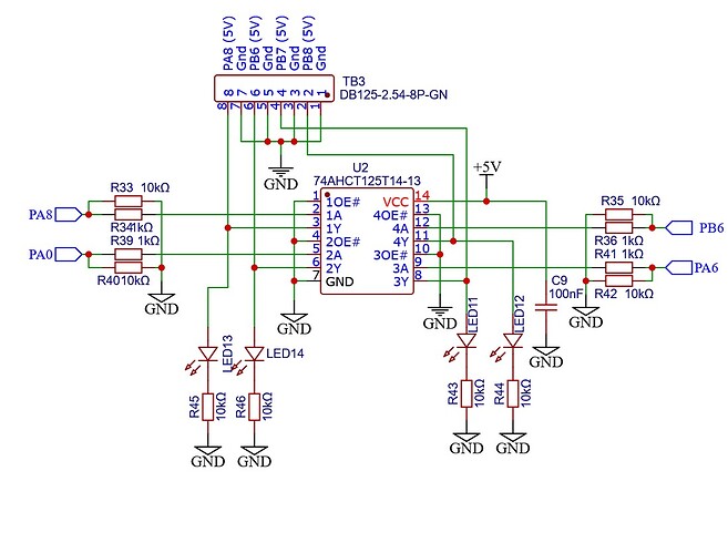
For Jackpot V2, I’m really leaning towards a recommendation that we take all of the available GPIO outputs (including the presently restricted / unused GPIO 0 ), and running them through a buffer/level converter. Expose the outputs of this. Then, run this over to the FET stage, maybe with a jumper to enable the additional FETs as outputs. If we want to keep the FET outputs as voltage selectable higher current rated FETs that remains fine.

Doing this means you could always hook up things like a “fast” digital signal (it isn’t fast) like a laser. You do that at the buffer/level converter point. Alternately, you could always hook up your 24V fan or your LED strip, or the SSR that runs your coolant or dust collection to those downstream FET output stages.

This is a little bit more expensive in part costs, but it does maximize the utility of the board as a general purpose integrated CNC controller.

1 Like

Indeed, and can get quite multi-faceted when considering things like inductive loads or significant inrush. The key thing is really leaving plenty of safety margin. The ability to use parts close to their ratings comes with a cost, and that cost is either a massive reliability question mark or a significant design-time investment.

There are a ton of different approaches here that could work, for sure. I don’t think I’m in a position where I can really recommend a specific approach because I still don’t feel like I have a good handle on what the V2 actually ‘is’, at its core, or maybe it’s that the goal has changed over the process.

So the best approach for me would seem to be to give a bunch of options, explain the pros/cons of each where necessary and then see where it goes from there.

That buffer from the jp1 has 4 outputs, I have no issues reusing that and adding gpio.0 as long as that does not mess with the boot/flash stuff again.

This would be 5v pwm/ttl If I am not mistaken, same as the jp1 5v outputs.

5v PWM to a higher level FET so we can get a higher amperage higher voltage PWM.
Breaking this in two parts to get one clean signal to the appropriate FET, instead of trying to get two FET’s to work with a 2.7v or a 17v signal. We know we will have a 5v signal and a 12-24v output.

Does not seem necessary. As long as it handles 12-24v the most common power supplies people would use, and we have a fast 5V PWM that gets everything I want…almost.

The only other thing I really want to solve is a better header solution. I am not keen on having 6 (8 if we add gpio.0 ) output terminals instead of the 3 (or 4).

Ever evolving, unfortunately. I am happy with the rest, I just want to make these 3 (or 4) spare pins do the most they possibly can. We now know at least 1 “fast” 5v PWM is required, I would prefer more.

Since I use these things all the time I just assumed it was simple.

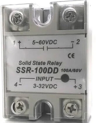
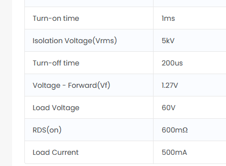
3-32v in, 5-60v out. Maybe they are not fast? I will look for a spec sheet for a surface mount version, I know I looked at them before.

So, thinking about possible approaches just to clear things up in my head because I’m a little blurry around the edges today:

The goal is we have 3, maybe 4 pins that can used as outputs and no real clear delineation regarding what those outputs need to do.

The simplest way would be to allocate 2x TTL and 2x high-side or something. Lowest cost, lowest design time, easiest verification, lowest board space used, least flexibility and poor utilization of a scarce resource.

Every output could have a TTL and high-side circuit segment running to different headers. Moderate cost, lowest design time, still easy verification, most flexibility, probably takes up the most board space.

Every output could have a TTL and high-side circuit segment running to the same header, selectable by switch or jumpers. Moderate cost, lowest design time, still easy verification, most flexibility, decent board space.

Every output could be a TTL output and have a separate part of the board that acts as a TTL input to high-side output buffer. Could free up some layout flexibility, moderate design time, easy verification, some extra flexibility in terms of being able to buffer external signals, moderate board space used, low-to-moderate cost. This would entirely depend on the implementation of the connection/routing choices. External wiring would be ugly and maybe lead to it just looking like it should be a separate board. Internal via switches or jumpers is basically just the option from above, etc.

1 Like

So that would work equivalently to what you’ve got, but is still only a single contact output and likely a very high capacitance one. You’d need a pull-up or pull-down to make a logic signal out of it and would inherently always have a slow edge.

I cannot imagine they’re super fast and may also have significant skew between rising and falling edges, so a turn-on may be delayed compared to a turn-off or vice versa.

There’s nothing in that module that would be much different at all to your existing setup… Edit: Aside from isolation, which can actually be a decent way to get high side drive, but you’ve got other options that are likely better there, anyway.

yup, too slow.

Agree, so far.

Where I am leaning.

It is funny, before this current issue. I never really ever considered speed. I just assumed everything we make is so slow it is never an issue. I assumed things we used in this space were relatively slow. Again, I hate learning with my wallet but dammed if I don’t really appreciate pushing my boundaries. And While I know this is still slow, I feel kinda cool that we are actually pushing circuit speed limits into question on this circuit kiddies projects!

1 Like

The thing is, there’s nothing inherently fancy about a circuit being ‘fast’… You can stick a 10c 74HCwhatever buffer on something and run it well into the 100MHz range or beyond. It’s not even that difficult, really, until you start getting into the more esoteric side of things like worrying about EMC etc.

It’s more about the breadth of the problem space that you need to solve for. By itself, things being fast, or high current, or high voltage, or long distance, or functionally safe, or EMC compliant etc. are all easy enough. It’s when you start combining things. Fast and long distance means you need a different approach and start heading towards differential drivers and twisted pair cables. Add EMC compliant into that and you go to slew rate limited drivers that are a bit more expensive. Add high current to that and suddenly it’s a weeks worth of design time or adding tons of extra parts etc.

I think you might be operating under the misapprehension that what you’re trying to do is easier because it’s flexible when in reality it’s the opposite! Every extra variable you add increases the complexity of the space you’ve gotta evaluate and opens up more pits to fall into.

10MHz SPI to a chip on the same board? Easy, just run a trace between the chips. 10A 24V drive? Sure, just make sure you’ve got the cooling sorted and trace widths correct. 1A 230V drive? Sure, isolation and check creepage/clearance, maybe consider the effect of fault current on a failure etc. Controlling something remote? Sure, just run a cable to it, make sure you’ve got some basic ESD/surge protection and filtering at either end and you’re golden.

Combine any 2 of those and it becomes 4x more complicated. Combine any 3 and it becomes 16x more complicated, etc.

1 Like

Actually, this is all worth it if we gain a 4th output pin. That is just awesome.

:hushed: Don’t burst my bubble, I was just feeling fancy!!

:rofl:


So the buffer from the arendale cost 30% less than the one from the JP1.

I am seeing a pulldown and current protection on the esp32 pins. That makes me nervous for GPIO.0. Can we leave it without a pulldown so it boots and flashes right, then specify :pd in the firmware for that output pin. I am guessing that makes this a flaky output but if it is used for non-critical things who cares if it blips on for a bit, (like pin 26 already does).

The esp32 gpio.0 boots high, low signals flash mode (it is tied to the boot button that pulls it down when pressed).

You declare right up front you can’t use it for things like lasers or safety interlocks

And the CP2102 handshake lines .

all fine as long as you use a high input impedance driver or buffer that won’t impact boot behavior. declare what the output can and can’t do as described above

1 Like

Done, io, 0 and 6 are for dumb stuff.

I guess I model it up, when the testers get here if :pd does not stabilize it, I just remove it. No harm in trying.


Anyone that has a Jackpot2, any feeling on the wago terminal blocks while we are making changes? I did see a removable screw terminal block on one of Bart’s boards that looks okay to me if you don’t like them wago’s.

1 Like

My point was more that trying to do 10kHz with a power circuit is in a lot of ways more difficult than trying to do 10MHz with a purely logic circuit.

Looks like that’s probably just down to it being a Diodes Inc part vs a TI part. They should be functionally identical, at least for most of the high level specs you’d be concerned with.

That’s a big ‘maybe’, but I very much don’t like doing that. Leaving inputs undriven can cause some wacky behaviour. I would sooner pull the pin in a direction that it needs, such as a pull-up, and then include a warning that this maybe glitch high briefly on startup so it should be used for low-stakes control like lighting or a fan, definitely not spindle control etc.

Another approach is that you can control the output enable line so that on boot the outputs are disabled, then it doesn’t matter as much that the inputs are floating. It’s still not ideal but it’s better. That would need something like pull-downs on the output as well.

They also don’t have anything between the logic output and the header which is something I dislike. Bare minimum there should be a resistor there, ideally resistor capacitor, even more ideally resistor, capacitor, ESD/surge protection etc. etc.

Edit: To clarify, leaving a logic input in an undefined state can cause worse things than just an undefined output, it can lead to it oscillating and max output frequency or drawing significant current. For a brief period on startup it’ll likely be fine, but it’s definitely not ideal.

At the very least I would consider trying to find out how much pull-down you can get away with. It may be that the ESP32 is ok with a 1Meg pulldown on that pin or something, which would still be a lot better than nothing given that the input leakage spec on the 125 buffer is 1uA, so 1MR should be enough to keep it defined to 0.8V or below in most cases.