Cam has a video to share!

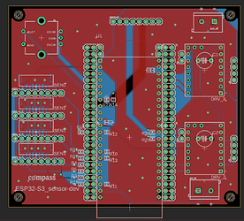
Ahhah I’m sorry Ryan, been away for the holidays working on boring computer stuff. New PCBs and a breakout board to test with ESP32.


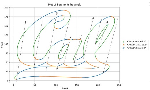
Also trying to finalize the path planning script that has been quite a bit tricky for me. This graphic shows how I’m planning to split up the passes for different orientations.

Now I just have to sort the groups of paths into practical passes for the machine to take. I drew little arrows on the graph output to show what this might look like for an arbitrary Cluster 0.

4 Likes

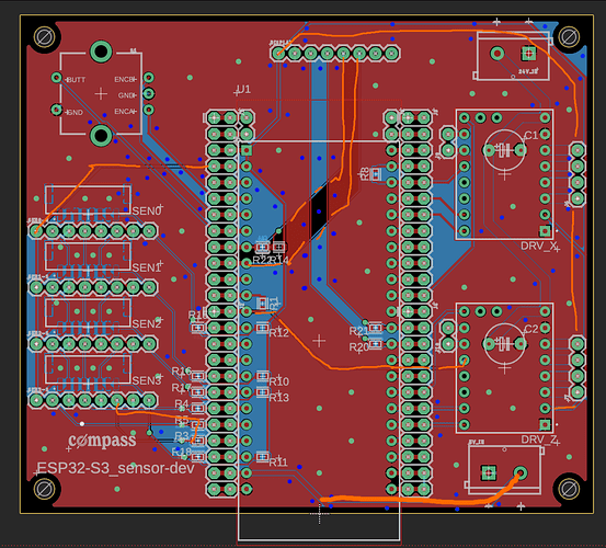
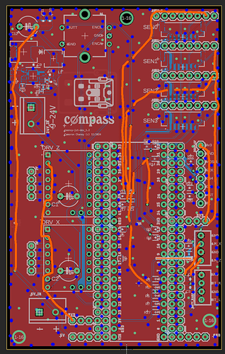
If you’d like a bit of feedback for future PCBs, I would suggest trying to keep as many traces on the top layer as possible and the bottom layer unbroken, even if it means more transitions to hop ‘under’ traces. I’d also include a lot more vias, especially to stitch under traces in the bottom layer.

I’ve drawn some suggestions here with the traces that I’d move or bring to the top layer in orange and then the extra vias in blue:

The goal is to try to provide a low-inductance path for the return currents in any loop. Any time you have a signal that has high frequency componnts, be it logic or power, there’s a high frequency return current that tries to flow as near to the trace as possible. Best case is that it can flow directly under the trace in an unbroken plane all the way back to where it started because then you have a small loop so minimal inductance which leads to fast edges, less EMI radiating off the board, less susceptibility to EMI from other devices. Worse case is that you have currents that need to go way out of their way to get back which opens up the loop creating more inductance which slows down edges, increases radiated emissions and picks up more noise.

Adding all the vias is basically just trying to give as many options for currents to change layers and take the shortest route. I typically cluster them around where discontinuities in the layer are like where traces cut through a pour. A via in the middle of an area likely doesn’t do much but near the edges they do a lot.

I’d also avoid routing traces hard up against the edge of the board if you can. These have the highest inductance/emissions/noise reception because they’re closest to a wire that’s just up in free space.

4 Likes

Wow thank you! I’ll definitely modify that to your points, along with the main board and sensor breakout board. Appreciate it :pray:

2 Likes

Oh cool, I had assumed that you had already made it.

Feel free to make a revision and then tag me if you’d like me to take another look. One of the coolest things about PCB design, to me at least, is that by learning a few basic rules you can improve the performance in so many ways like making them more robust to external noise etc. without changing anything other than the copper shapes on them. In some cases you can even make the overall product cheaper by needing less filtering components or allowing use of lower performance components etc. simply by improving the copper layout.

3 Likes

Should 4 layer stack-up instead of 2 be used if routing high frequency signals? Not sure what would be considered high frequency requiring this, but, thought using 4 layers enables an internal ground layer for return path being physically much closer to top signal traces.

Personally appreciated info in related PCB design questions topic.

2 Likes

It entirely comes down to the complexity of the design. A 4 layer board will almost always perform better than a 2 layer board in a bunch of ways, but what that actually means in practice will vary. Plenty of designs out in the real world still end up being single layer for cost purposes. For hobby stuff 4 layer is insanely cheap now but still usually more expensive than 2 layer.

The key thing is what is ‘high frequency’. A design with 1ns edges and multi-GHz clocks will have significantly different needs to something with 100ns edges and 20MHz clocks etc. Having the return path closer is directly an inductance consideration which is then a frequency consideration. There’s also the significant factor of how much high frequency (and what, again, high frequency means) bypass capacitance is needed for the rails which can only really come from PCB plate capacitance, not from lumped elements.

Almost everything I design is 2 layer unless I can avoid it. My current project at work is 6 layers because I’m having to land a pretty meaty fine pitch 256 ball BGA, but aside from that it’d be doable in 4, potentially 2 with a larger board at very little performance penalty.

4 Likes

Having Jono here helping with the board is the best that can happen to you board-wise. He did some major Jackpot magic. :slight_smile:

6 Likes

So much great information! Just finished reading through that PCB design thread and have a few more videos queued up to learn more hahah. This return path stuff is super interesting. I’ve known vaguely about it with ground plane practices and whatnot, but to actually use it to intentionally decompose signals is wild. I’ve always just thrown them on the PCB kind of hand wavy. I definitely have to read up some more that. Lots of stuff that I still don’t understand hahah.

And will do for sure! Thanks so much.

2 Likes

I often feel the exact same way and I’ve been doing embedded hardware and power electronics layout for a couple of decades now!

Anything by Rick Hartley is good. Eric Bogatin is good. Henry Ott, Ralph Morrison. High Speed Digital Design: A Handbook of Black Magic by Howard Johnson is amazing. I haven’t been through it recently and it’s a bit old now though physics hasn’t changed so it’s likely still mostly relevant. Anything by Keith Armstrong (emcstandards.co.uk, Cherry Clough Consulting) is amazing, I was lucky enough to do his entire 1 week product design/EMC/EMI/testing course earlier this year.

One of the key things to remember with all these guys is that they’re approaching this from a commercial designer standpoint where often individual costs aren’t an issue, it’s overall optimization of costs to reach a specific goal, i.e. a robust, reliable, manufacturable and standards/EMI compliant product. Following all of their recommendations would of course be great, especially if you use this stuff in your career but fundamentally I disagree with a lot of their perspectives when it comes to DIY/amateur projects. A lot of this simply isn’t important when using free/cheap tools to get a single or handful of widgets working. It’s important when you need to go as quickly as possible from design to high volume manufacture without delays due to EMC testing failures and subsequent PCB revisions or when you’re trying to design defensively to prevent excessive in-field failures or warranty/loss of customer confidence related costs etc.

That’s where I think it’s useful to consider the 4-layer point that @azab2c is bringing up, which is a great one to think about. That takes a 100 mm x 100 mm PCB from $5 to $25 at PCBWay. Not really that much but if you assume you’re not likely to get it right the first time and might need to take another stab at it and then may want to revise it again in the future to add more capabilities as needed, that’s $15 to $75… Then it’s a case of what those 4 layers are actually getting you.

If you’re putting modules on the board, like it looks like you are, those modules themselves are already incredibly compromised from an EMC/inductance perspective so it’s kinda like trying to supercharge a golf cart. It’s fixing some issues, but even the best layout and PCB stackup in the world is going to be hampered by the fundamental fact that you’re at the mercy of the modules above. You don’t need to worry about the DC supply impedance because even if you put massively high performance DC capacitance on your board, it’s going to be wasted because of the inductance between that board and the devices on the module itself. The module is the only realistic way to address any of those issues. Same thing with overall signal integrity. It doesn’t matter how good it is on your board, the limiting factor is likely to be whats on the modules, the inductance of the pins going up to those modules and the insane amount of inductance added by the incredibly poor pin layout of most modules (think about where the nearest ground or power return path is for some of those signals, we’re trying to keep them closely coupled within < 1-2 mm and they’re in some cases 10s of cms away.

So all of that’s a long way of saying it’s awesome watching Rick Hartley’s stuff and trying to understand more deeply the topics he’s talking about, especially when it comes to things like how return path energy distributes and why different stackups and layouts are better than others, but it’s similar to watching a Titans of CNC video and then trying to apply the techniques discussed to machining aluminium on an MPCNC… The physics is the same, but it’s SUCH a different league that it’s not really all that applicable and can even steer you wrong. The worst case would be that it leads you to waste time on minor tweaks leaving less time/motivation to address potentially bigger issues that these experts assume would already have been taken care of. Watch it, by all means, but try to keep some perspective in mind. If he’s talking about frequencies in the 10s of GHz, that’s well sub-ns edge rates. An ESP32 on a DIP module is going to be lucky to do 100ns, for instance.

4 Likes

Super valid points, thanks for the reminder to keep perspective. It can definitely be easy to lose oneself in the details sometimes and forget that it might just be a drop in the bucket for what is actually being designed. I do always love to learn these things, though!

As for the specific signals that I’m dealing with on my board, I’m curious if you’d have any input as to how much care I should put into various aspects of the design. My main concern is with the four sensors, which are all communicating on the same SPI bus (50ns rise times at 2Mhz serial clock frequency). SPI is already super sensitive as is, and I am using wired connections for each of them, 20cm-40cm long. I’ve already seen issues with crosstalk in previous PCB designs which causes the sensors to misbehave. So I’ve been implementing a few things in subsequent designs to help mitigate this. I’ve added 100Ohm series resistors to the SPI lines to reduce capacitance, added extra ground lines in the cables for current return paths, and started using CAT8 ethernet cables (not sure if CAT8 is overkill, but I definitely feel more comfortable with everything shielded…) with each signal line in a twisted pair with either GND or VDD. I’ve also been trying to keep the higher voltage power lines and signal lines separated as much as possible on the PCB, as well as keeping a GND line between the signal lines for long runs.

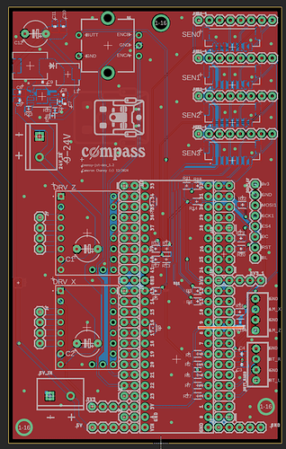
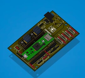
This has been working well so far, but it’s hard to tell how much more I should be digging in, or if I’m overdoing it in certain areas - like maybe I could get away with CAT5 instead of CAT8 cables. This is what I have for the main PCB right now for reference (though there are already a lot of things I want to change from your previous feedback!):

3 Likes

The 100R resistors won’t help with reducing capacitance but they do significantly reduce the peak currents created by driving fast edges into those capacitances, which will in turn reduce magnetic field around the traces and reduce crosstalk accordingly. It also slows down the edges a bunch which helps with removing the higher frequency components that are most affected by issues with return path.

2MHz is suuuuper slow, so you’ve got a ton of leeway to increase that resistance and slow down the edges further.

Adding extra ground lines is a good idea, especially in things like ribbon cables/flex cables and between sensitive/high EMI traces. That helps to control that return current to being in a lower inductance path and a path that doesn’t share its inductance with the other traces around it. In something a bit more mixed like a bundled multi-core cable it will still help but not necessarily as much because you don’t have control over exactly which cables are grounds or not without some careful forward planning and specific cable selection.

Cat8 is likely dramatic overkill and I doubt it’ll do much for you there, relative to the cost/complexity to implement properly.

I generally think that shielding is a LOT less valuable than people think, largely because it’s difficult to do well and so I think it’s often more of a security blanket than something that actually improves a design. Ethernet is a great example of this. The shielded connectors for ethernet are hot garbage. They don’t connect well to the shielded plug, they don’t connect in enough spots, they don’t offer good shielding all the way to the PCB, and the plugs have a very poor connection to the cable shield as well.

On the other hand, differential signalling is a LOT more valuable than people think, which is where almost all the robustness of ethernet and other comms signalling like RS485, CAN etc. comes from.

That’s probably what I’d try to go. It’s not differential so it will have limited benefit but it’s probably the most predictable, performance wise, and should be differential-enough with the highest frequency components. I’d stick with that, I just wouldn’t worry too much about the actual Cat rating of the cable.

Definitely don’t worry about keeping them separated by a significant amount. There shouldn’t be any significant high frequency content on your power lines, that’s why you should have good decoupling caps at each power supply node. I don’t typically see any issue with routing power directly adjacent to signal lines.

I don’t really bother with this and I certainly don’t run ground signals at all, instead I try to keep the bottom layer as clean as possible and then visually check it to make sure it’s continuous and I can ‘see’ what I think will be a valid high-frequency return for each critical signal. Keeping space to allow the ground pour to spread between high edge rate signals can be a good idea but it’s seldom something I’d feel the need to prioritize, especially at the frequencies mentioned above.

A better approach to all of that is to control your edge rates to be as low as you can get away with and work from there. Having resistors close to each driver output is a good idea then tuning those to match the parasitic capacitance to get an edge rate that’s as low as possible but still acceptable.

Typically issues with crosstalk aren’t about the signal conductors at all, they’re about poor/broken return paths that force huge amounts of mutual inductance between adjacent traces.

I’m about to head out from work but I’ll take a look at that PCB later tonight or tomorrow and let you know. From a quick perspective I’d try to do the same things I mentioned above: All traces on top as much as possible, more vias, especially near slots in the top/bottom copper pours, trraces routed away from the edge by at least 1mm, that kinda thing.

3 Likes

So from taking a look at that 2nd board, the same things as above:

  • Try to keep traces on the top side as much as possible. There are likely to be some real crazy return paths there because they need to go around the long parallel or perpendicular traces on the bottom side
  • There are a few traces along the edges, try to avoid that if you can. A good rule of thumb is to try to have a ‘via wall’ around the edge of the board. Having copper top and bottom and a row of vias around the edge is a technique used to avoid ‘edge fired’ emissions from multi-layer boards, but it can also be a good catch-all rule to avoid doing anything ill-advised with routing paths.
  • I would avoid routing traces in a plane you’re going to pour, it’s making some of the thermal reliefs look really weird. Not really a functional problem but it does immediately draw the eye and ‘look wrong’. I try to encourage people to have things look predictable and uniform because it makes it easier to spot issues. If I’m constantly seeing things that look weird, my eye is drawn to them and I need to use mental effort to dismiss them and move on, rather than having my eye just drawn naturally to things that look wrong and are an actual problem.
  • My approach to 0V plane connections is that I will highlight any pads connected to 0V and make sure that each one is a through-hole or has at least one via right next to it. If you’re concerned about the thermal reliefs being too small, try find a way to adjust that on a per-pad or per-net basis, Altium has pad classes and net classes you can use for adjusting automatic rules like that.
  • More vias! They’re free :smiley:

Another thing I thought of with the SPI is that you only really need to worry about crosstalk between the SCK lines and the MOSI/MISO lines. The crosstalk typically happens with the high frequency content that occurs in the edges which are only on state changes. A MOSI edge change causing a glitch in the MISO line won’t do anything because it will settle back to normal before the SCK edge. A SCK edge causing a glitch in the MISO line means the glitch occurs at the same time that the state of the MISO line is read causing potential corruption. The other lines like nCS can have something like a 100pF/1nF capacitor on them at the device end meaning any crosstalk/noise will be reduced significantly and we don’t need the chip select line to be high performance.

As for slowing down the edge rates, I would add an RC filter (which can also easily be tried as an LC filter using a ferrite bead) at the driving end of each SPI line, so one at the controller on SCK/MOSI and then one each on each device’s MISO, taking care to avoid the total capacitance getting too high if you have a ton of SPI devices. I would start with just the resistor fitted at 100R as you have and leave the capacitor DNI’d. The nice thing about that is that you can then add the capacitor and change the resistor if you need to as a problem solving step. A 100R resistor and 20pF of trace/pin capacitance should give a rise time of around 5ns, so isn’t likely to affect much as the controller is probably slower than that in most cases. With good layout, you shouldn’t see any disturbances even on directly adjacent lines, but if you do then the next step would be to either increase resistance or add capacitance. Adding capacitance will increase overall current consumption but lowers the impedance of the trace to any external noise. Adding resistance slows the edges without increasing current consumption but will raise the impedance of the trace which can lead to more issues with noise/susceptibility. Going to a 100R/100pF would give 100R/120pF total which is a step response of 28ns so ~100ns to do a full transition. I would be reasonable comfortable until that total transition time is close to 1/4 cycle, so ~250ns. Slower than that and you might not have the signal completely settled by the time the clock changes state. Too slow and you can also have issues with triggering multiple edges in some chips (ESP32s for instance seem to have slightly temperamental/glitchy GPIO inputs).

I would also typically add a resistor/capacitor at every single connection off board (0V included) as a matter of course. You can easily fit them as 0R links to start with or the same 100R edge-rate limiting resistors as before for signals but it gives you a place to fit ferrite beads and low-value capacitors as a form of noise/EMI reduction. If you want to get really extra you can rub-out the 0V plane under a section that covers the connectors, the resistors and the traces between them. That limits any high-frequency signals coupling from those connections straight into the 0V plane and ensures that whatever series impedance you add to those lines has the highest blocking impedance to the highest frequencies. A common mode choke can be better for higher frequency signals where you don’t want anything slowing them down but want to avoid conducting common-mode noise into the board, but most of the stuff I end up dealing with doesn’t really need it, honestly. I put it on fully differential signals like CAN, RS485, Ethernet (you usually get that for free in the magnetics package) and those are normally my highest frequency off-board signals, anyway.

Controlling this stuff is kinda why you ideally want anything off-board to be either slow and single ended or fast and differential. Noise and external interference tends to couple into all the conductors in a cable equally so it’s much easier to brutally filter the common mode noise signal while leaving the high frequency differential signals relatively unscathed. Shielding is always an option, of course, but unless you’ve got them extremely well filtered at either end or the shield well connected to a conductive enclosure at both ends then the shielding quickly loses its effectiveness. It’ll still help somewhat, but it can be surprising how little a non-ideal shield setup can actually reject!

2 Likes

As I did before, orange lines for traces I’d move or bring to the top. Blue dots for extra vias, might have gone a liiiiittle overboard there…

1 Like

Maslow 4 uses RJ45, which seemed like a cool way to leverage existing easy to source and install Cat cables. But… For Maslow 4.1, looks like design is switching away from RJ45 to instead use JST-XH. Not sure if reason(s) are vibrations, EMI and/or something else(s).

Thank you so much for taking the time to give such detailed feedback! You’re learning me a lot in this little case study.

Happy to hear. I’ll stick with CAT5/CAT6 for my new device and see how it goes.

Oh interesting, I guess that makes sense since the nCS isn’t actually sending data?

Yupp good thing the SPI communication is pretty slow for this board then. I have a lot more leeway than I had originally thought. I had also considered doing a CAN connection to the sensor boards, with some sort of CAN-SPI bridge to interface with the chips. But I could imagine there being a lot of extra wizardry that would have to go into that. If the SPI works reliably with a simple RC filter and cheap, standard rated CAT cabling, then that’s cool by me. Would be an interesting thing to explore, though.

3 Likes

Yes, I was actually talking with Bar about this! That’s part of the reason I wanted to go with JST instead. Because the RJ45 connectors only have a single point of contact, any dust from cutting would cause the connections to fail. JST connectors have multiple points of contact, so they should be more robust in this regard. JST-GH connectors specifically are also designed to be very robust to vibrations (often used in hobbyist drone flight controllers like the Pixhawk), so they make a lot of sense for CNC applications.

2 Likes

This is definitely possible and CAN is a lot more straightforward than most people think, but it also suits some applications more than others.

CAN is fundamentally great when you’re passing specific realtime information back and forth like sensor values. To start with, each frame is defined as an address plus 8 bytes of payload and then a transmit frequency. This could be something like saying address 0x170 is going to be the Current Position frame, contain X, Y and Z positions as 16b signed ints and be sent every 100ms. That would make bytes 0-1 be position X, bytes 2-3 be position Y and bytes 4-5 be position Z. Endianness isn’t specified so I would usually just do whatever makes the most sense for the controller I’m working with to make decoding the message efficient, but ultimately it probably doesn’t matter. You’d then go through and define a bunch of messages like that, maybe another one for spindle RPM, one that could be less often for temperatures and slow changing values. Lower addresses have priority during the arbitration process so you use the lower numbers for critical data that needs to be transmitted reliably and higher numbers for things that can handle variable latency and slower delivery. We also usually try to group things such that each frame has all the information needed to do some kind of specific device or decision, so potentially the position could also have endstop status, the spindle details could have fault bits, relevant temperatures, power measurement etc. There’s also an ACK bit which indicates that at least one controller has received the frame correctly. If you have multiple controllers you want ACKs from it’s sometimes better to sent multiple frames, one suited to each controller etc. or handle that separately.

Where CAN gets a bit weird is where you have existing data that doesn’t fit well into specific messages, you’re trying to bridge generic bulk data or need to transmit a lot of stateful information. It can be done, such as having a message that’s just ‘here’s another 8 bytes of serial data’, but it’s not really a great use case and adds a lot of complexity/overhead for no real reason.

CAN can also be less robust than expected in some cases. It’s kinda weird in that it’s not actively driven as marks/spaces, it’s a dominant/recessive bus more like one-wire, where one bit is signalled by all the controllers just leave the line to float to a passive state while the other bit is actively driven that way. That’s what allows the the automatic arbitration and means you don’t need specific controllers/masters on the bus. The passive state means that it can end up being a lot less noise-immune if you’re not careful because the bus needs filtering that’s appropriate both for an actively driven low-impedance state and a passive higher impedance state. Still miles better than anything that isn’t differential, but with potential traps.

Some of the SPI CAN controllers can be a bit limited in terms of the throughput and number of messages they can handle, so I generally try to avoid them in favour of hardware that has on-board CAN peripherals.

Personally, my preference is to head towards something like RS422 for replacing serial links when I need something robust. It’s a lot more straightforward to make bullet-proof when needing something that just looks like a UART at each end.

Ok that sounds super doable. I currently have more than 8 bytes of data (I think 12 bytes) being read from the sensor for each time step, but I could probably take out some unnecessary values, or just split that up into multiple frames. How do you usually initialize a sensor read from the master side in this sort of interface? I would also probably have to allocate a byte for the address of the sensor doing the reading too, huh?

Yeahh hmm my use case might fit into the “trying to bridge generic bulk data” category. Maybe it’d be worthwhile to look more into RS422 in the future.

I’d typically just send everything that might be useful but have some frames that are less frequency informational ones. It can be a bit annoying keeping the frame definition updated, although if this is just a point-to-point link then that’s less of an issue. Once you’ve got half a dozen different devices on a CAN link all sending different stuff at different times from different code bases it can get a bit squirrely.

In general, it’s easiest to add data to a partially full frame, 2nd easiest to add a new frame, hardest is to reshuffle an existing frame and change data order etc.

So typically I would try to avoid statefulness as much as possible. If you want sensor data every 100ms then I would just have the thing that’s doing the sensing just start up and free run, sending it every 100ms. If you have something where sometimes the sensor data isn’t valid, I would either set up a state code that can be sent along or a set of flags. Something like a byte that can enumerate to Normal, Error A, Error B, etc. Or if it’s just a set of conditions, each could be a binary flag like Running = true/false, Overtemp error = true/false, Initialized = true/false, homed=true/false etc. Picking what to do there is usually a case of what you’re trying to accomplish and is usually obvious which is most suitable. If there are only a couple of binary states but without any commonality then flags are easiest. If there are a bunch of specific states where only one can exist at a time, a byte with specific numbers for each code would be best. If there is a mix then it could be something like Running = True/False, Error = True/False and then a separate error code, 0x00 no error, 0x01 overtemp, 0x02 overvolt, 0x03 etc. etc.

If you’re trying to control something, having a message that’s from controller to sensor that has a command flags or a command byte also works. The easiest/cleanest is to have something that makes sense to be sent repeatedly over and over, like Command = Run/Stop/Init, etc. and then step through the states on the controller according to feedback. You can also treat it as something that gets sent once like you send a single message that says ‘Init’ as the command to trigger an initialisation but that’s a little bit ugly. I would prefer to do it as something where you constantly send the command and then track the state on the sensor side.

Yeah, you’ll need separate messages for controller to sensor and sensor to controller.

So as an example if you had something where you were controlling a CNC machine:
The CNC machine could have a frame that it sends that has a bunch of flags for initialized, homed, moving, error and then XYZ position. It could have another frame that it sends for spindle state which has RPM, error flag, spindle temp.

The controller could have a frame that it sends that is a command byte and then 7 payload bytes according to the command. It only sends that frame once per command but needs to receive an ack. It could instead have a fixed frame that it sends a command byte, XYZ position, spindle speed all crammed into one frame. Doing it that way you could have a ‘no command’ message which is just spammed to be ignored. That would give you ACK feedback constantly without sending things. You could do it such that you send the command as ‘Home’ once and then no-commands while the machine is homing. You could do it such that you send the command ‘Home’ constantly and the machine knows to start homing when it goes from any other command to home but then ignore additional home commands beyond that, etc. etc.

It’s all just a case of thinking through the flow of how you want it to work and trying to consider all the ways it could tie itself in knots (like the controller sends the Home command constantly, the machine tries to home, sends a ‘homed’ flag once it’s done, receives the Home command again and re-homes, so the system oscillates) or miss a certain combination of conditions then plan for those. It’s best to make it inherent, if possible, such that a sudden drop in messages or a stuck message won’t break things with the 2nd best being to program in special cases to handle weird conditions like the repeat homing thing etc.

Another thing you can do is choose whether you want in-band or out-of-band error signalling etc. Like for instance if you can have errors for each axis you could do them as a set of binary flags, errorX, errorY, errorZ. You could have a single byte that’s just ‘error’ and has error codes like 0x01 = errorX, 0x02 = errorY etc. That gives you the option for more information errors (like X overtemp, X undervoltage, X unexpected home trigger, Xmax limit, Xmin limit etc.). You can do in-band signalling like having valid positions for Xpos be 0x0000 to 0xFF00 and then having errors be 0xFFFF, 0XFFFE etc. That can be a nice and efficient way of transmitting those errors, but it needs a lot more care to avoid mistakes like having an error that’s a valid negative position in the case of an unhomed movement or something where a value gets checked whether it’s in error, gets updated in an interrupt to go from a valid position to an error and then gets processed as if it’s a valid position etc. etc.

All depends on your goals. CAN and RS422 are a great pair of technologies to be familiar with because they accomplish the same thing in vastly different ways. If you want something that’s basically a robust serial port, RS422 is awesome. If you want something that is just shuttling numbers around and the protocol/checksum/acknowledgement/arbitration is all handled for you then CAN can be great.

There’s also a lot to be said for using whichever one seems the most interesting to learn about!
2 Likes

Indeed hahah! You’ve ignited a little fire in me, might just do them both…kidding :eyes:

2 Likes