Can always roughly design both and go with whichever you think suits best. I’ve got tons of things I’ve designed over the years and never built or never finished, but I learned something from each of them.
True, true. Very likely possibility!
1 Like
I designed a lot of CAN communications in robotic trucks. I prefer sending a bunch of state periodically than any kind of send/respond. It just fits better with the CAN protocol. So you never depend on one message to get somewhere. One micro might be sending a bitfield with states related to idle, running, alarm, initialized, etc. The second might be sending values for X Y Z, etc.
For a sensor, Ideally it can fit everything into one 8Byte message. And just send everything all the time. If it can’t fit in one, then Ideally it can be split logically so each message stands alone. It would be less than ideal if X was in a separate message than Y, because they might be slightly out of sync on receipt. You could put stuff like error state in a separate message than XYZ position. Or play games like having a base position and then a more frequent offset from the base position to fit everything into smaller messages.
You should also use intel endian (little endian) if you have to cross a byte boundary. J1939 does that and that made it pretty much the standard for CAN. But you can do what you want.
It’s fun. But definitely trickier than SPI.
5 Likes
Gotcha! Sounds simple enough. I’ll mess around with that when I have time, but I’ll probably just stick with SPI for now while it works
1 Like
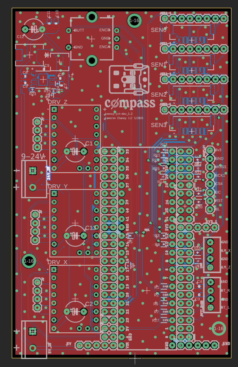
Got a couple new PCB revisions. If you’re still up for it @jono035 , I’d love to get your expert feedback! Pretty much moved all the traces to the top, moved them away from the walls, cleaned them up, and added a bunch of vias. Just realized I forgot to put in DNI capacitor placeholders for the SPI lines - might add those in too.
6 Likes
Yeah, for sure, happy to take a look. What package are you doing that in? If it’s something online like EasyEDA can you send me a link? Bit easier to look at the higher resolution versions!
Sure! I’m working in Fusion 360. The shareable links are kinda weird so lmk if there’d be a better way to view the layouts:
If you have Fusion you can also download the project and open the layout, schematic, etc. in the app.
Fusion has that?
You should give EasyEDA a shot. I picked it up pretty quick and having the parts library and easy ordering from JLC is pretty slick. I like seeing prices and quantities.
Yup I just started using Fusion’s PCB design because I used Eagle before. I do have to admit, EasyEDA seems pretty awesome for it’s connection with JLC. I’m always kinda thrown off by the browser interface though.
The only real benefit of Fusion electronics I’ve seen (other than my familiarity with it) is how seamless the 3D footprint integration is. It makes it real easy to do super precise custom PCB outlines and enclosures.
1 Like
They have a native program if you prefer. I have very little PCB experience but it did everything Jono told me to do!
Yeah drawing squares in easy eda is fine but importing shapes takes a bit if trial and error.
I do find it super fun to do though. I want to do a basic redesign of the Jackpot now that I understand more after selling a bunch.
2 Likes
Well, I’m always lurking about somewhere or other if you’d like a hand with any further Jackpot stuff.
3 Likes
It’s definitely weird to be reviewing it all in the 3D view but it’s working well enough for the moment!
That’s a worthwhile reason. I’ve usually done enclosure design by exporting a .step file but it really depends on how nicely the CAD package works with a large .step file with potentially thousands of embedded smaller models. EasyEDA having a solid parts library behind it with component links for ordering is a huge benefit.
As for the PCBs:
That bottom layer is SO much cleaner now. There are a couple of odd things that might be worth checking out:

It looks like the thermal relief setting results in more clearance than the rest of the board, so those 3 grounds are only connected via the 2 spokes at the end and the middle pad is only connected via the top layer. In situations like this it can sometimes be better to shift the thermal reliefs to 45 degrees if the tool will handle that, rather than 90 degrees because that’s usually where an adjacent pad is.
How are you having these boards made? If they’re being commercial made/reflowed then the thermal reliefs don’t matter quite as much. I often turn them off for mounting pads like the JST connectors so that they have a bit more strength. All that’s holding them to the board is the glue under the pad so they’re very easy to knock loose. I would typically flood them with copper and then put a couple of vias around them as ‘rivets’ to keep them down. I’ve never specifically tested how effective that is, but it makes me feel a bit better about them:
Something like this:

The main thing is to make sure that the hole of the via is 0.1-0.2mm away from the edge of the solder mask opening. That way you won’t get scavenging which is where the solder gets wicked from the pad down into the via as it’s melting, leaving the pad without enough solder to make a good joint. That’s also solvable by having the vias epoxy filled or plugged but that’s usually a higher cost/premium process in case you want to put a via in the pad for space/performance reasons.
What’s the clearance and trace size you’re using? For boards that I’m not trying to cram a ton of stuff into I typically default to 0.2mm/8mil for traces and clearance with 0.25mm/10mil for polygon clearance. That used to be a pretty reasonable standard that could get your board made nearly anywhere without them complaining but these days that would be extremely conservative, so just using 0.2mm/8mil for everything is probably fine.
I would still go through and try to get a via as close to every single ground pad as possible, ideally right next to where the spokes of the thermal relief are.
I’d also consider flooding that thermal pad in the middle of that IC. In general having a thermal relief on a pad that’s intended to provide cooling for a device is counterproductive. The thermal relief makes it easier to solder by majorly decreasing the thermal conductivity to the surrounding plane which in turn ruins the effectiveness of the ability of that pad to conduct heat away from the package and out into the plane to be rejected out to ambient air. It’s a tricky balance sometimes as making a pad have better thermal performance inherently makes it harder to solder. If you’re using reflow to solder it then it typically doesn’t matter because the entire plane will be heated evenly by the reflow oven, regardless of thermal reliefs. It’s only really hand soldering with an iron that benefits from thermal reliefs.
That’s from a ‘will it end up soldered or not’ perspective. There are still some arguments to be made about the rate of heating on small components. With small 2-pad passives like resistors and caps I typically try to keep the copper connections looking similar on either side. If one side has a tiny 0.2mm trace going into it and the other side has a direct connection to a copper plane that can in theory make it more likely for one side to flow before the other leading to ‘tombstoning’ type failures. That’s where the solder on one pad flows before the other and the surface tension leads to the component lifting up vertically. In reality I don’t think I’ve ever observed any real trend in that way. When watching our hand-assembled boards in our convection reflow oven at work, all the pads tend to flow at the exact same time, regardless of copper. I presume because the airflow is heating all of the copper evenly and larger copper structures that have more thermal mass also have more surface area which evens the effect out, etc.
Some ‘visual’ comments below. I don’t think any of these suggestions would be the difference between working or not but they hopefully help with developing good routing technique which in aggregate can make significant improvements to the performance of a board for zero cost other than the time spent to spot how to make the improvements.
One thing that a lot of PCB designers try to avoid are acute trace connections. The stated reason in the past was that acid could get stuck in tight corners and over-etch but I personally think that’s a bit of a myth, at least with modern designs. Regardless, it has stuck out as being the ‘standard’ from a visual perspective.
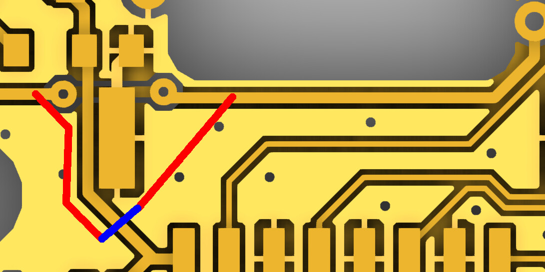
Stuff like this: Instead of coming out of the side of a pad like that, I would route these out from the corners instead. It doesn’t have to be 100% perfectly out of the corner, just enough that there isn’t that acute inside angle on the edge of the pad.
This is how I would typically route traces out of that shape of pad:
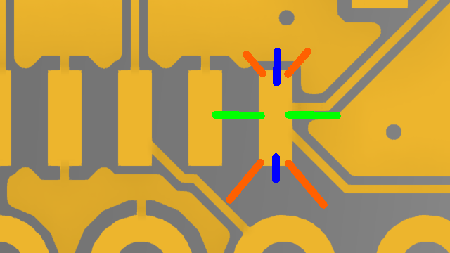
My first preference would be the blue traces, so 90 degrees directly out of the short side. The second would be the red traces out of the the corners, the last would be the green. Ultimately it would still need to be the best option for whichever way the trace is running off to, so I wouldn’t use the blue option for any of the traces on that pad because all they’re going to have to do is turn to head away from the pad anyway, so the corners are what I’d use.
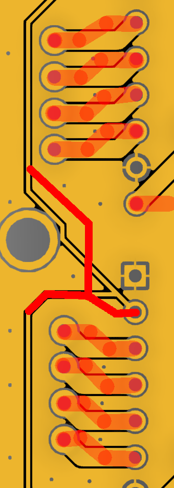
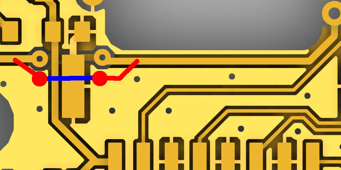
Another thing is that you’ve got a bunch of traces that you’re routing point to point between pads. In some very high frequency circumstances this is a good idea but that’s typically if there’s a termination resistor at one end. For the frequencies you’re talking about here it may be cleaner to route things like this:
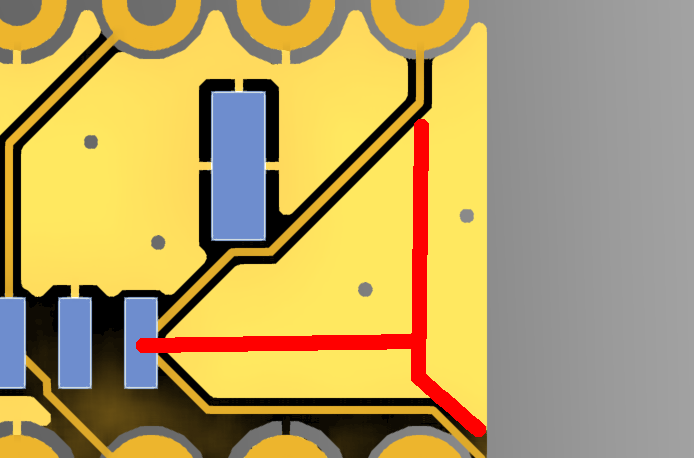
It’s also a nice idea to, where possible, route things such that thermal reliefs like the pad above are as full as possible. Even just pulling that trace down slightly will allow the ground plane to fully surround that mounting pad and give it all 4 spokes without any other penalty. The same thing goes for the power trace on the left side of that connector. It could be routed straight vertically between the through-hole components and then stubbed off to the JST connector without issue.
As above, routing at 90 degrees out of the long side of a pad is my least preferred option but in this case it’s where the trace is going anyway so I’d live with it.
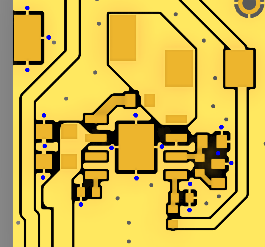
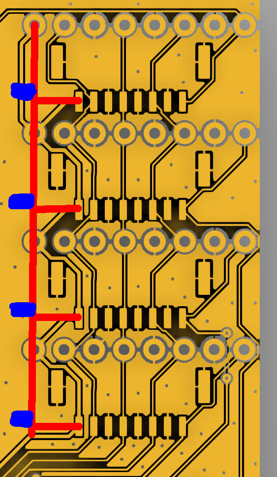
I can’t remember what those connectors were for but I remember discussing the SPI bus and that looks like it. I would at the very least add 100nF decoupling caps to the power connections, usually one per connector routed as close to the connector as possible and in-line with how it’s fed, but with a bunch of connectors like that having 8 of them probably doesn’t do that much more than just having a few spread along there. Perhaps 4, spread along that length would be good, something like the blue blocks above.
(I think there might already be these resistors here at least, without seeing the schematic it’s a little difficult to figure out what’s what and where, so potentially ignore this if it’s already done) As we’ve discussed before, something like a 100R series resistor and 100pF capacitor on each data line, depending on operating frequency, can give some options for helping with noise immunity, too. That does start to get a little packed in there when it’s that tight, though. Having one set towards the bottom of that image above that is for all of the SPI headers could be a simpler but still potentially useful option, given that it’ll still slow down the edges on the clock, MOSI and nCS lines and at least do some work controlling the return path for anything on the MISO lines, even with significantly higher inductance than an individual cap. So for each ‘outgoing’ line like SCK, MOSI, nCS I’d do Microcontroller - 100R resistor - 100pF cap to ground - connector and then for the ‘incoming’ lines like MISO I’d do connector - 100R resistor - 100pF cap to ground - Microcontroller. 100R/100pF is a ~16MHz corner frequency so shouldn’t have much effect on a 2MHz SPI bus. I’m usually a bit lazy so typically I’d just open LTspice, make a 2MHz square wave voltage source, put the 100R/100pF RC network in front of it, probe the result and eyeball it to see how ‘square’ it looks. As long as the rise time is ~10% of the pulse width then you’re fine. You can also do that mathematically by using an RC filter calculator and seeing that the rise time is 23ns, 2MHz period is 500ns so pulse width is 250ns, that’s around about right.
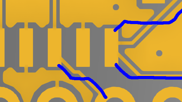
With sections like this, I’d try to shift the routing so that it can allow the ground plane to flow ‘around’ the pins:
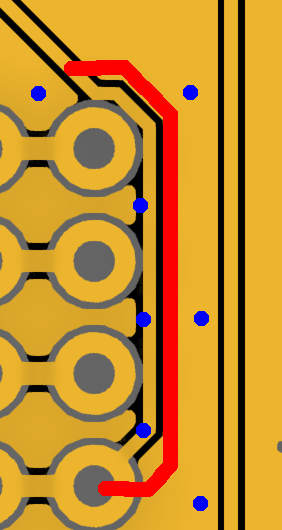
Without doing that you’ve got an island of copper and then 3 little copper fingers sticking out between the pins. They look like they’re ~10mm long, presumably, so that’s a 1/4 wavelength antenna at 8GHz or 1/8 wavelength at 4GHz. That’s well in the range of frequencies that the board will be subjected to, especially with an ESP32 floating nearby and they will quite effectively pick that up and re-radiate it which can cause issues. Instead by allowing enough space for it to turn into 3 slots that are ~10mm long instead which significantly raises their resonant frequency, essentially for free. Alternatively, you could add vias towards the tip of those fingers which will also stop them being nice little whip antennas. I would probably do both, something like the blue dots above.
There are a few places around where some tweaking to traces can easily allow the copper to web together more cleanly. As I said above, none of this is remotely a ‘you need to make this change’, more just 'this is a good thing to look out for and can usually be avoided for free.
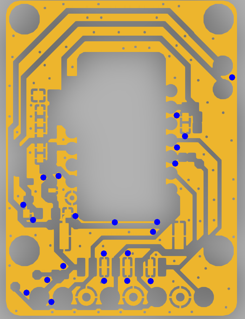
I’m not sure how Fusion is choosing how to group the bodies in the 3D view, but I can turn off pretty much everything except the top layer copper pour. That’s a good way to look at it to see where extra vias could be used.
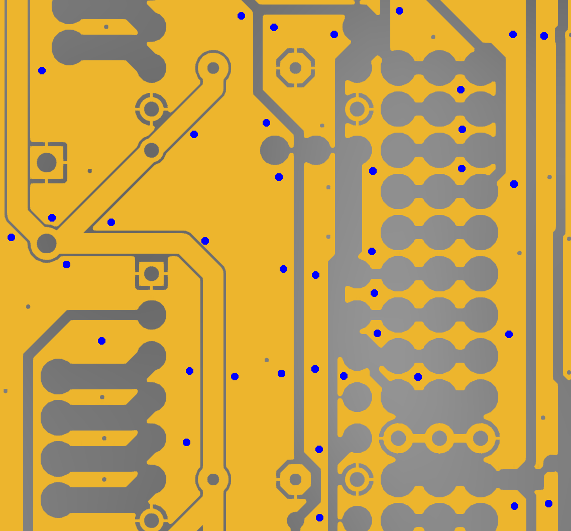
Looking at that view, you can see some pretty big areas of copper without vias, as well as some more copper ‘fingers’ that don’t go anywhere. I’d add vias towards the end of each ‘finger’ you see and try to make sure there’s a via within 10mm of others, etc. Also thinking about having them as ‘stitching’ down the sides of traces helps a bit, too. With such a clean ground plane on the back side this isn’t critical at all, it’s another good habit thing. I usually try to keep the copper webs as complete as possible while I’m routing, then once everything is routed I’ll go back and take another look over to see what can be improved/cleaned up then once I’ve done that clean-up is when I’ll pepper vias all over the place. It usually only takes a few minutes of just clicking around everywhere. Then take a step back, take a look at the board with only one layer at a time visible and only the ground highlighted or visible to try to spot anywhere I’ve missed of that looks suspiciously open.
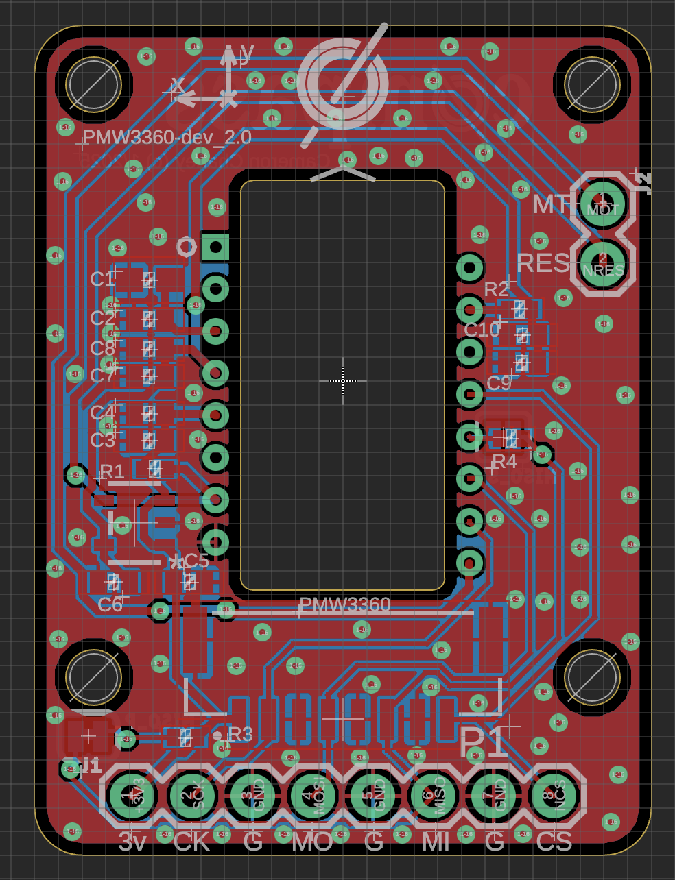
For the 2nd board, same thing with the thermal reliefs, the clearance around them is way larger than I’d use leading to some pretty big holes in the plane and some weird routing.
On both boards there are still some ground traces that are getting poured over. I’d avoid that unless it’s doing something like fixing a mucked up thermal relief that you can’t fix in any other way.
Same thing with the thermal reliefs on the mounting pads for the connector, might be better to pour directly over them.

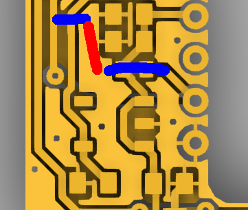
What’s going on here? Could that same thing be done with a 0R link or solder blob on the passive above?

Similar here? This looks a little odd, what’s this part/

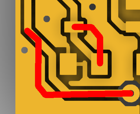
I’d try to find a way to break up the top trace here as it’s forcing all the return current for any signals to go around the plane to the left. It only affects a few signals so it will depend a lot on what they actually are, but it will increase the mutual inductance and crosstalk between those quite significantly. It looks like you’re jumping 2 traces there. One option is to do that in 2 jumps, something like this:
Where blue is the trace on the underside and red is a new trace on the top side.
Another option is to specifically put vias on either side of the trace to the copper on the top side to create a ‘link’ over the top, like this:
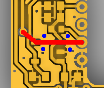
Where the red is just showing where the trace runs on the underside and the blue vias are to create the ‘links’ over the top. Ultimately that’s probably worse overall than avoiding the interruption in the bottom plane. The bottom is mostly pretty clean which is great, there’s just those small couple of things that can be improved.
Another improvement would be to shorten the other little dogbone on the underside or at least move the righthand via down slightly to thicken up the copper web around it.
That would be an option for shortening the bottom side slot.
That would be an option for increasing the web around the top right of that right hand via. I think either of those are probably fine.
I would also move that larger trace down or make it thinner so that some vias can be placed in that thin sliver of ground plane above. That’s a nice long whip antenna so it should be connected to the plane below with a via or two or removed.
Do those thicker traces need to be that thick? A 0.2mm trace is good up to about an amp and a 100mm long 0.2mm trace only has 0.2R of resistance. It can be easy to fall into the trap of thinking something like ‘this trace carries more current so it needs to be thicker’ when in reality it’s the difference between 100uA and 10mA. Both of those currents are perfectly fine in a 0.2mm trace and there’s often no reason to thicken up a trace. That chip looks like it draws a max of 40mA steady state, 70mA peak which is well within the range of a 0.2mm/8mil trace.
Overall it looks good. There are a few spots where some extra vias would be nice.
Changing a few little routing things like this:
Would help with fixing that slightly dodgy thermal relief on that pad and allow a closer ground via.
8 Likes
Their downloadable version seems to just be a desktop client for the website… Idk I’m probably making too big a fuss about this aspect of the software. Seems like it’d be pretty decent
Thank you so much! This is amazing.
Good call. I’ll add in those via rivets too. I’m using JLCPCB for the manufacturing.
I’m using a 6mil min trace (for the SPI lines, 12mil for the other signal lines) and 6mil clearance. I’ve used these spec for boards in the past and JLC has had no issues with it.
That makes a whole lots of sense.
I’ve been told before that routing traces with 90 degree angles is a no-no, because of the EMI emissions? Is this a myth, or maybe something that only applies to very high speed designs?
Yup, I had the series resistors on there and just added the capacitors as DNI. They fit in pretty nicely actually near the board pins. I’ve never worked with spice software, but that could be a fun thing to dig into.
Oh shoot, that’s wild! The accidental antennas always catch me off guard. It’s a pretty cool (but also pretty annoying) phenomenon.
That’s a jumper I added for initial development when I wasn’t sure if I needed the series resistor or not. But yes, you’re totally right that the same thing could be achieved by replacing the resistor with a 0R link or a solder blob across. Would those be preferred? The other weird part is the same concept, but with the connection NC for a pull-up resistor on the MISO line.
Phew, think I implemented all if not most of those changes! Thanks again for that detailed review. It’s such a pleasure learning from an expert in the field.
3 Likes
Yeah i really agree! Love having @jono035 around here! So much fun to see that side of things!!!
Thanks for all you do Jono!
6 Likes
I wouldn’t bother changing sizes of lines by task unless necessary. I typically use 0.2mm/8mil everywhere and then drop below that for short distances if I need to squeeze between 2 pads.
In general it’s best to keep a little bit away from the minimum. If JLC say 6mil is the smallest then I’d use 8mil for most where it doesn’t matter and then only drop to 6mil for small sections. The minimum is usually the thinnest trace they can reliably get continuity on so a nominal 6mil may be 4mil or less in parts and often the etching leaves the trace being somewhat trapezoidal, too, so it won’t necessarily have the same area as a 6mil x 1.4mil square. If they say 4mil is the smallest then 6mil everywhere is probably fine.
By that same token, there’s not really anything to be gained from going bigger, especially not in a design that’s in tens to low hundreds of mA of current draw. It makes rework a bit easier if you need to tack a wire on somewhere, I guess, but beyond that it doesn’t do much.
That one has been around a long time, from memory I think it’s technically true but such a minor consideration as to be a myth for anything realistic. If you’re routing for 40GHz radar, maybe, but for even 500MHz clock signals I don’t think I’d worry. I also think it’s more of an impedance discontinuity issue rather than anything else, so can cause reflections in the line rather than specific radiative issues. Personally I stick with 45 degree corners everywhere because I think it looks nice. Trying to keep the design to having traces lined up and with even spacing, 45 degree corners with the ‘bevel’ part similar lengths etc. all looks like a design where someone has taken their time to make it look good. I don’t think that helps the design in any way and may actually be technically worse in some cases (traces too close together leading to crosstalk is an obvious one). On the other hand I believe that if something looks the way you expect, it’s easier to spot discrepancies because we’re amazing at spotting variances in patterns. One example is not joining traces in a + shape. If you offset them and use two T shapes instead it looks deliberate, where a + looks to me like an autorouter was used and had an error. In reality there’s no performance difference but if I’m looking at the + and trying to consciously decide ‘is that correct?’ then I’m using the limited resource of my attention span on something meaningless, rather than spotting the poorly formed thermal relief next to it that is only hanging on by a tiny sliver of copper.
Yeah, honestly that’s the kind of insane beauty/terror of EMI/EMS design. Everything is an antenna. Everything radiates, everything receives, it’s just managing stuff so that the things you don’t want to radiate are crappy antennas and the things you do want to radiate aren’t.
0R resistors are awesome, people should be using them everywhere. They’re technically not as good as a trace but only in ways that are irrelevant below the GHz range and you’ll even still see them used there. The great thing about them is that putting them on does nothing to your design but gives you the easy option to add a resistor, ferrite bead, diode, whatever later so they give a ton of flexibility to a design, whether deliberate or accidental. I couldn’t count the number of times that I’ve done exactly what you’ve just done, put pads on for an RC filter and only fitted the R as a 0R link then changed the design to be an RC filter, an LC filter with a ferrite bead, a peak-and-hold circuit by using a diode instead of the R, a diode on the C to prevent undershoot, stand an R and C up next to each other on the C pads to make an RC snubber etc. etc. The only downside is they take more space than a blank trace but then the upside is they’re like having an extra PCB layer for a brief period. If you have 2 traces that need to cross over one another, it’s likely better from an EMI perspective to add a 0R link and route one trace under that 0R link than it is to drop it into your return layer.
Depending on the size of the components used, blobbing solder across them works pretty well but I just make sure I’ve got 0R resistors in every kit we use. If you get a component kit that doesn’t come with them, usually the smallest value will still work just as well, like a 1R or 10R. Even on a lot of power traces if you’re careful and have a properly sized decoupling cap on the far side. But I’d just recommend getting some, anyway!
You’re most welcome! I really enjoy seeing people give this stuff a crack, especially given that it’s so incredibly accessible. The free tools like EasyEDA are better than the $10k tools I started using and being able to get a $5 PCB from PCBWay/JLC is insane compared to the $50-80 I used to pay at the low cost supplier we used to use let alone compared to the $200-400 from a local supplier.
3 Likes
Making me blush! In all seriousness, I really can’t express enough how much I appreciate the kind words and how much enjoyment I get from seeing people get interested in the details of this stuff.
I like it here. It’s a far cry from the professional or more electronics focused groups (cough EEVBlog forums cough) where it’s more likely to see someone arguing, trying to tear people down or discourage them from participating if they don’t meet some magical hidden criteria.
6 Likes
I’m not sure if I’ve mentioned this but typically a formal review process would start with the schematic before layout happens. Often we’d go:
Preliminary schematic review - This would be a way to catch larger issues early, especially ones that lead to significant re-designs like changing filter types, using different components, maybe adjustments to the product requirements documentation even. This could involve a number of disciplines such as component engineers who will have insights into a parts reliability or lifespan, manufacturing engineers who will know which packages/technologies are preferred for which types of design. Mechanical engineers might have feedback on part types from a cooling/mechanical mounting standpoint, etc.
Designer goes away and makes the changes recommended
Final schematic review - This would result in a finalized ‘accepted’ schematic design that can move forward to layout. Often there are still changes recommended but they’re usually simple enough that they don’t need to be reviewed again or maybe would be ‘spot reviewed’ via e-mail or whatever. A junior designer would probably have this as an entire 2nd review process. A senior designer would probably be trusted to just make those changes and move on.
Designer starts placement
Placement/mechanical review - This is where things like connector placement, mounting hold placement, board shape/size, fitment into the enclosure, clearance with other components, wire routing considerations etc. would all be checked. This would also be the start of EMI considerations because components need to be divided into EM zones, connectors placed so they can be filtered well etc.
Designer makes changes to placement/board shape and starts layout
Layout review - This is where we’re at now, it’s the first review of the layout and would typically focus on things like I’ve mentioned above, good layout for EMI, correct trace width, clean return planes, via locations, clearances between EM zones, space for shielding etc.
Designer makes the layout changes.
Final layout review - Depending on how many changes were needed and how severe they are, as well as the reliability of the designer, this could be a spot review or skipped altogether.
Board goes out for manufacture.
That might seem like a bit of a crazy process but once you’ve seen a few nightmares it starts to make sense. I like it because it’s a bit more of a ‘review early and often’, where each thing could be 15 minutes to half an hour and avoids significant backtracking. In a professional setting it becomes pretty rare to have a ‘this will not work, you need to do X’ kind of issue, it’s usually more like ‘that has a minor risk of X happening, Y would mitigate that’. Things like provision for filters/ESD protection on lines, multi-padding components to account for potential supply issues, etc. Everything is a tradeoff so it’s usually things where maybe it could be 1% or 0.1% of assemblies could have that issue and that issue could be a slight reduction in performance, so any changes need to be weighed against the time it takes to change them. Making those changes at the layout stage sucks especially as boards get more complex because you need to rip up tracks, move components, potentially even change the board shape or connector positions etc. etc.
It adds time, for sure, but there’s nothing slower than a design that needs a revision or that has an issue that takes time to identify. The craziest one I’ve seen personally was an ambiguous component value on a BOM where a capacitor wasn’t called out as being critically important and a tiny 0402 C0G capacitor got substituted for a much cheaper X7R capacitor of the same capacitance and voltage rating. That caused the design to work fine for initial testing and then a couple of months later start failing when tested at extended temperature ranges, leading to a several month effort that tied up a couple of engineers and lead to buying another thermal testing chamber. Probably a total cost of half a million dollars just in lost productivity, let alone the truly horrifying costs that can rack up when a project starts to run behind by months. Stuff like that kills companies!
Obviously none of that necessarily applies here, but it’s worth explaining the ‘ideal’ process so you can decide where there is the most value to be added by review. For instance if you’re working on something and post up the preliminary schematics, it’s way easier to suggest adding things like filters or series resistances, ESD diodes, extra capacitors etc. up front at that point rather than later. There are also a whole bunch of things that I cannot comment on. The layout you’ve got looks good and with those changes should be better from a signal integrity standpoint but no amount of signal integrity will save you from having Rx/Tx wired backwards or a component that has its footprint made upside down accidentally (remarkably common!).
3 Likes
Loe the peek into the professional design process! Definitely seems like a lot, but I’m sure it prevents a lot of headaches in the future. I’ve only had very minimal experience designing PCBs in a professional setting (simple one-offs for R&D groups), but I’ve definitely experienced the benefit of a detailed review process for mechanical engineering projects. It can be so easy to get tunnel-vision when working on a design and forget something super important that could be fairly obvious to someone else. A second or third set of eyes really makes a world of difference.
3 Likes
Maybe just go full hovercraft.
It’s an old post, so also apropos with the necro-reply …
I first read this as “Maybe just go full Lovecraft.”, and wondered if Eldritch powers or non-euclidian geometries would help, given that I doubted abject racism was the call.
1 Like