Pendant Development

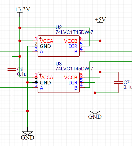
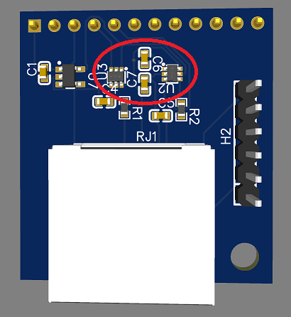
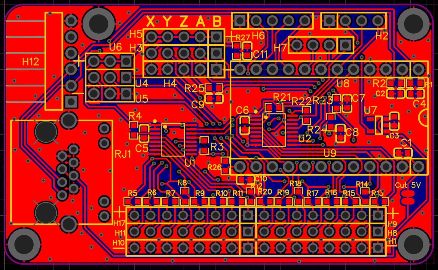
I would definitely use one decoupling cap per translator IC. The goal is to have one capacitor as physically close to the power/ground terminals as possible (ideally within a mm or 2, 5mm total ‘path’ length) so that the higher frequency components of a fast edge rate will be supplied from that capacitor, rather than from one further away down a higher inductance path that will cause the supply voltage to drop briefly (or the ground node to rise briefly) on transition. It’s a geometric consideration more than it is an electrical/schematic based consideration. If you end up with 2 decoupling caps that are basically right next to each other than you could remove one, but I wouldn’t bother. 100nF capacitors are probably the cheapest and most commonly made part on the board, so they’re likely less than a cent each.

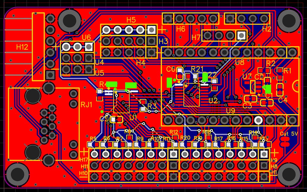
I would also use decoupling caps every place that there’s a VCC signal going out on a header, typically. Partly for decoupling, partly to filter any noise from coming back down the cables and into your supply lines, which isn’t that different of a purpose to decoupling, really. For the banks of headers like H1, H16, H5 then I’d just put a single one there.

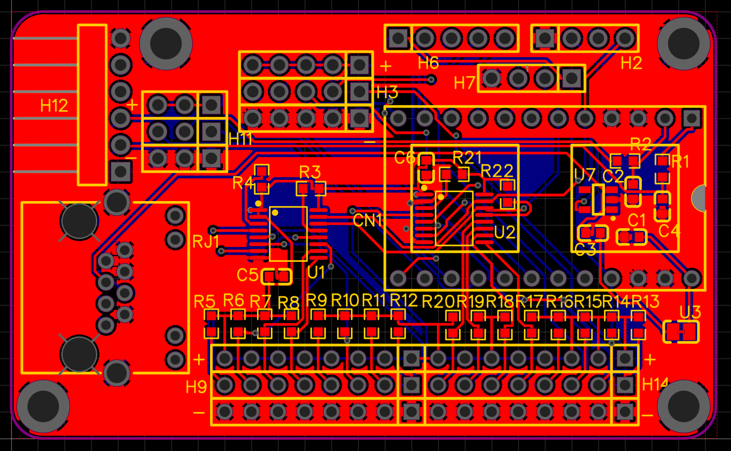
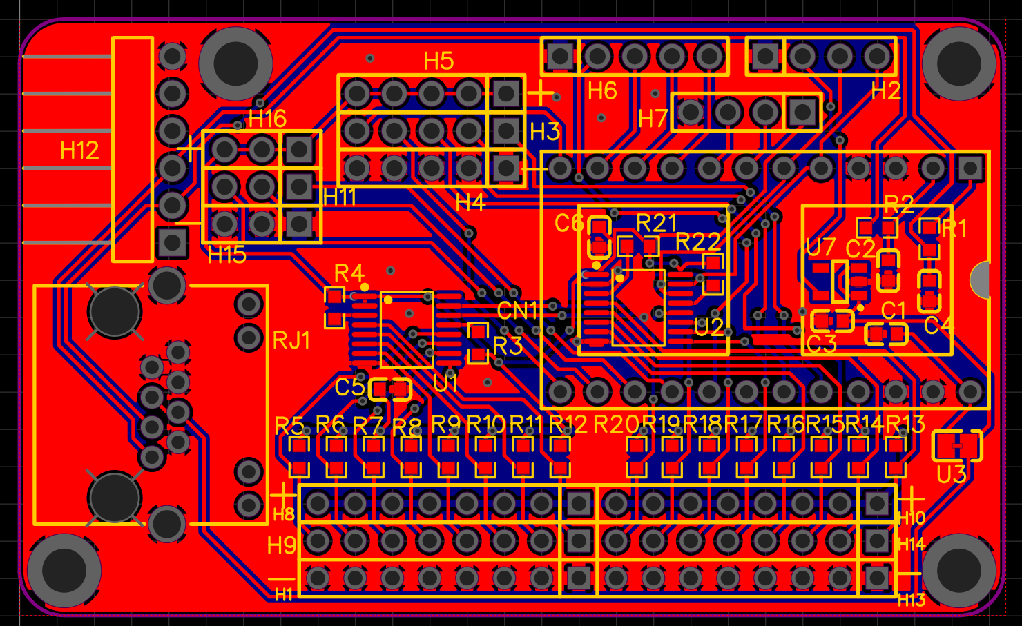
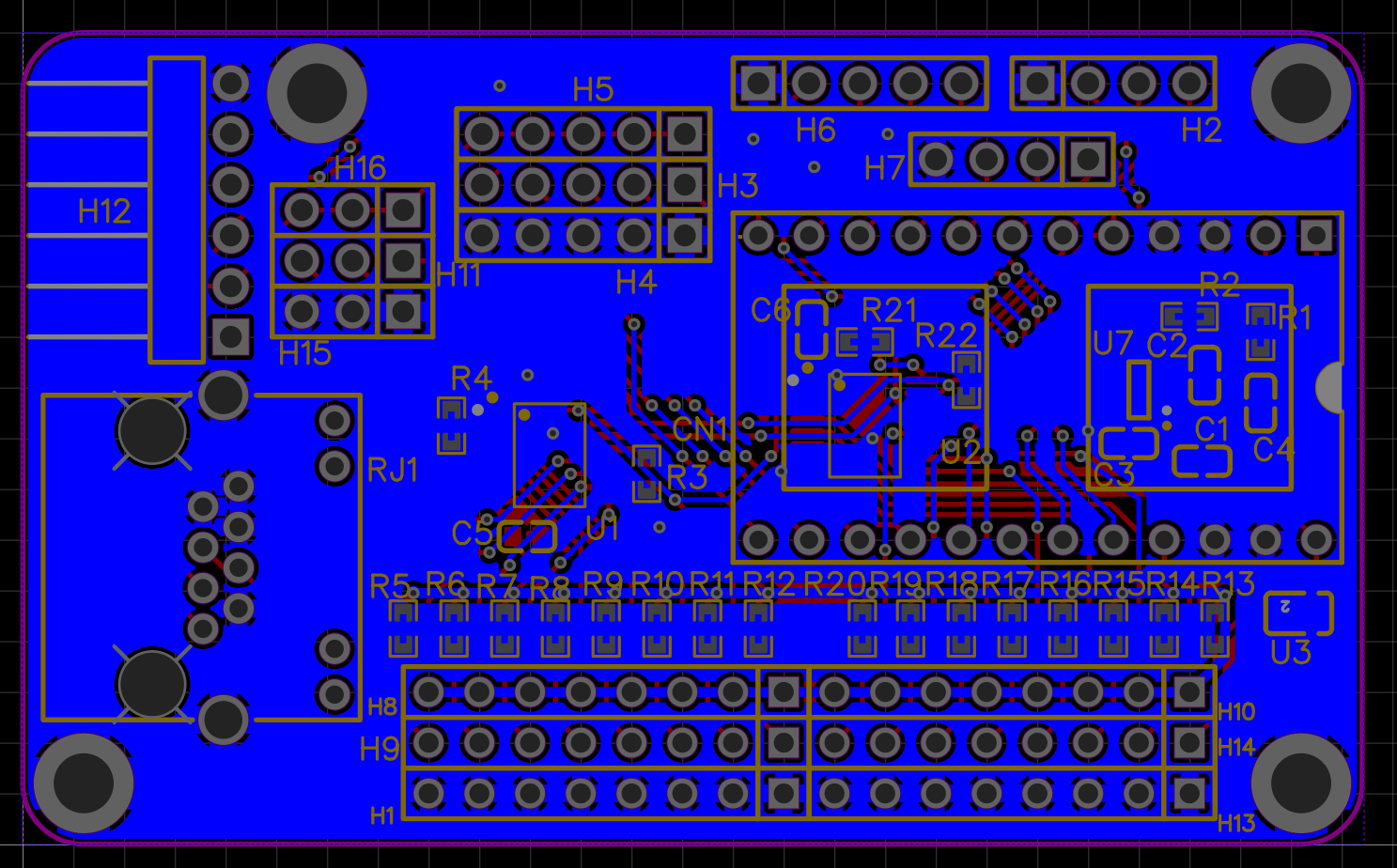
Just a weird thought with the layout of those headers, in future I’d probably do them as 8 instances of 1x3 headers to closer match the ‘intention’ of their use. That way you’re guaranteed that each header will be the correct dimensions because they’re a single part, you’ll have flexibility to move them around a little if needed and it will make the schematic much more readable, which is key to avoiding mistakes. I wouldn’t change it now. It’s baking my brain a little, though.

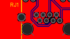
With header H6, where was that heading to? I’ve lost the plot a little bit with this design, sorry. I ask because it doesn’t currently have a ground net routed to it.

Was this just a test to see how it turned out? Auto-routers typically turn out designs that are ‘maybe’ DC correct but almost never good enough to actually attempt to use, in my experience.

I would always strongly, strongly encourage things to be hand routed. On simple boards it may not matter, but the only way you can tell whether it matters or not is by getting the boards back and testing them. Signal integrity failures are the worst to debug and will just be ‘the board works fine most of the time, then it doesn’t’. These are the failures that can soak a lot of time to find.

The other thing is that on simple boards, you might as well use those to develop the skills needed to do more complicated boards. I would have said that the pendant board already has enough routing on it to be quite complex to do well in a 2 layer board, just due to the number of traces.

This will also give you a feel for what the tradeoff is when adding extra stuff to soak up unused pins and how to do it effectively. Adding block headers like that is great for functionality, but it adds a lot of routing complexity. If I’m not sure I’ll use it, I’ll typically add them as single through-hole test points. That lets me wire something up manually if I need to use them and then I can add the proper hardware in a future revision if needed, without making the planned-for design significantly worse.

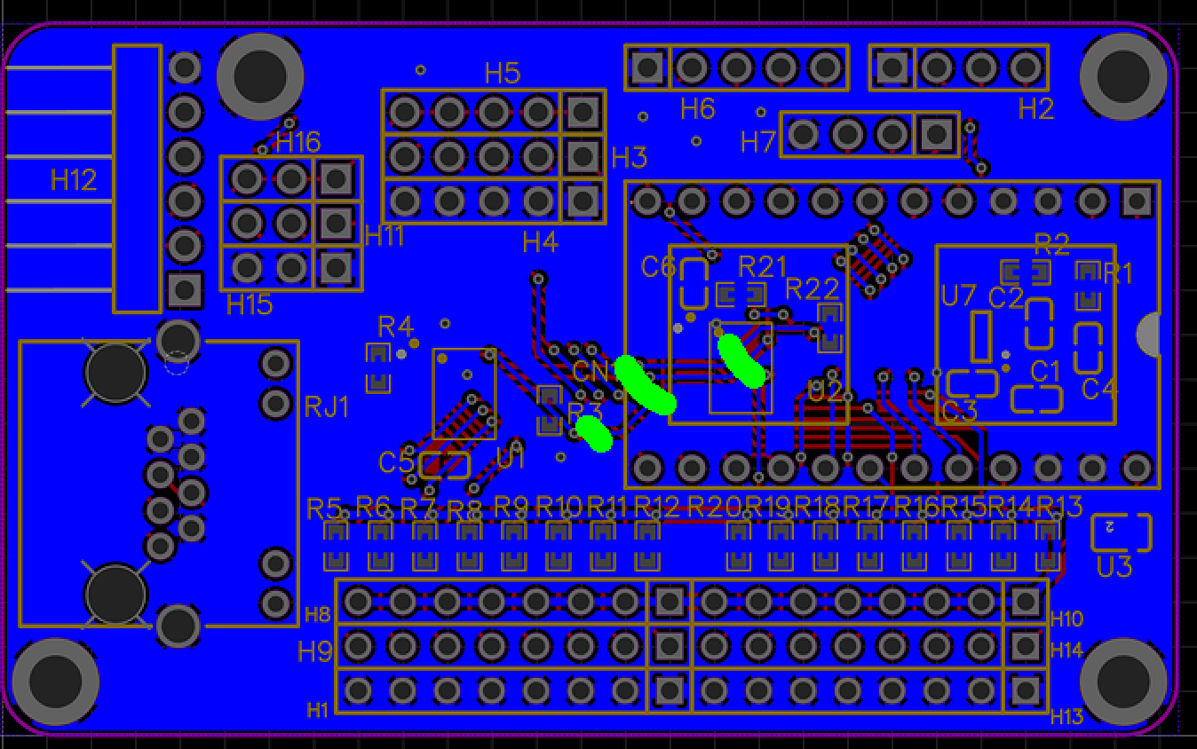
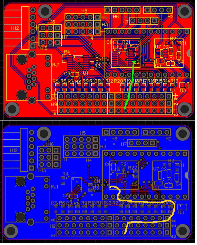
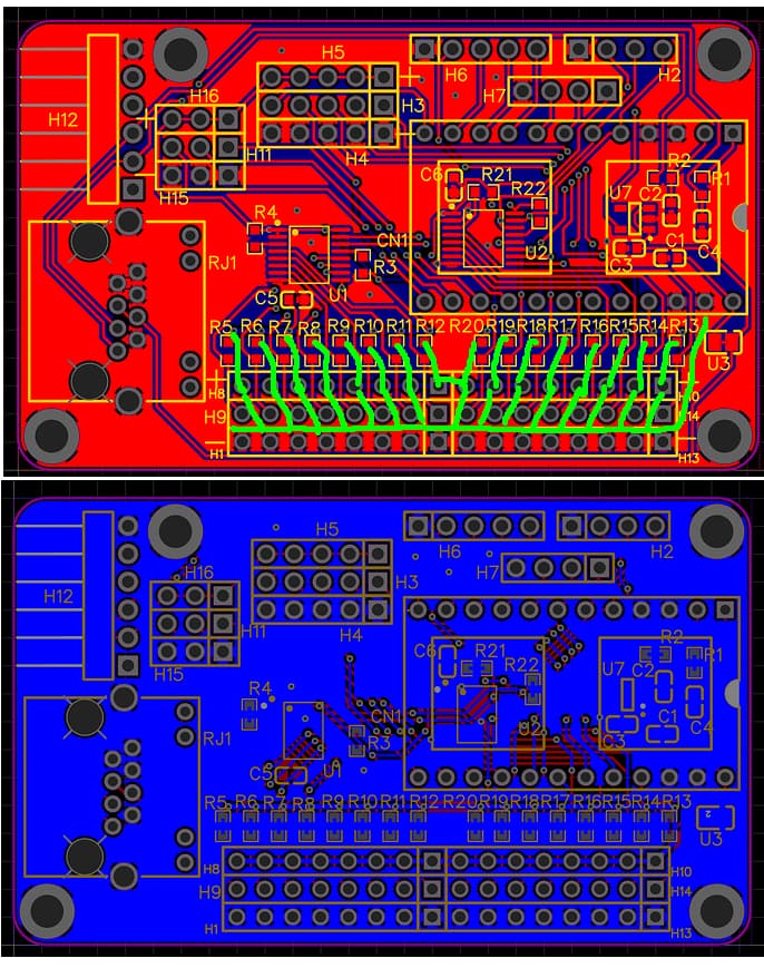
In terms of the issues with the above board, it comes back to the same stuff I was writing about in the 6-pack thread. For every single signal, you should be able to go through and draw a loop for where the current will flow. Even digital IO signals will have current flowing because input pins have capacitance, so every time a signal changes state, a small high-frequency burst of current will flow between the input and output pins on a net. That current will also have a closed loop path back to where it came from. The goal is to make that path as low inductance as possible, which we do by making the loop area as small as possible. Looking at some of those ground traces, the loop area is huge, which means that any current in the loop will radiate off the board and cause noise in the adjacent loops, as well as any noise externally (like a brushed router that’s basically a broadband noise generator, for instance) will be picked up by those loops like they’re an antenna.

My approach to routing a board like that would be to forget about the ground connections for the moment, try to route all the signal connections cleanly first, then get all the power connections routed, then go through and pour a ground polygon on the top and bottom layers to provide the power/signal return path. Try to keep connections to the top layer wherever possible. If you need to use the bottom layer, try to do it for brief hops then come back up to the top so you’re not cutting ‘slots’ in it. Try to group signals together so that you can get big unbroken chunks of ground plane. Then add vias everywhere that you can.

Other than that, is looks pretty good. I would also try to move all the designators on the silk layer so that they’re not touching any other silk and so that they’re not over the top of pads. I also try to keep them all the same orientation as the component (where it makes sense), as well as all in one of 2 orientations, so that they’re all either 0 degrees or 90 degrees for instance.

3 Likes

It is really awesome to see the terrific spread of talent in here! Bravo to you 2!

5 Likes

If the commands were “interruptible”, then you wouldn’t need this.

If you can say, “Go X+10mm” and then after it travels 5mm say, “No, Go X-5mm” or “stop”. That would also work. You need to make aure the user can change directions quickly. Your solution is to not send commands far enough in the future for the user to notice. My solution is to abort commands mid-execution.

I think grbl does the latter. But I may be mistaken.

Getting position feedback would also be nice, in case you also wanted something like a DRO. It is frustrating to me that gcode is so “standard” and the feedback messages make no effort to be standard at all. Marlin has some trouble computing real time position updates. But still, the format is 100% different than grbl. And neither standard is generic enough.

1 Like

Ok. I can easily add two more caps for the one-per-IC (per supply) rule but I’d like to learn if this is a valid exception.

This part of the circuit is the two single-signal voltage translators:

Which is this part of the layout:
image

They are already pretty close to the ICs and I could double the value just as easily, instead of making two adjacent capacitors. My other thought was that each level shifter should mostly only draw from one of the supplies (I guess that’s an assumption about how they work internally), so they are not doubling the load.

To be clear, I’m not arguing for one capacitor per IC (per supply) per se, I’m just wondering if my thinking is wrong.

I had hand-routed boards in the past in Eagle CAD entirely for fun, like a game of Tetris, but the problem is that the criterion for success was whether I can cram in all the stuff and obey the DRC. I don’t know if the signal quality is any good. I don’t know if I can effectively develop skills if there is not a “signal quality score” feedback that I can optimize. That would make it like a game again and I would have a chance.

My other thought is that everything is pretty low speed and low current, so I’m hoping a “DC” layout is going to be pretty decent. I want to be mindful of not getting “stuck” on optimizing too much, and I feel like this is entering diminishing returns, so I think I will proceed as-is, though I did clean up the silkscreen a bit and filled with ground planes top and bottom:

The 3D render showed silkscreen over top of the solder pads which seems strange to me. I don’t know if this is real or if the manufacturer will maintain solder pads clear from silkscreen, but anyway I moved them so all the pads are clear now.

H6 is a rotary switch to select between “off” and “Wheel X”, “Wheel Y”, “Wheel Z”, and “Joystick”.
H2 is OLED, H7 is encoder wheel, H3 is analog XYZ and two knobs, and H12 is for the FTDI. I don’t have a dedicated port for selecting between low/medium/high jogging speed, but I can use some of the 19 available generic pins for that.

There is definitely merit to this and I think in my skimming I had read something about Grbl maybe doing this. Marlin has no way to modify the queue except for blowing everything catastrophically, so for Marlin the choice was made for me.

I think there may also be a difference between an analog joystick and an on/off fixed rate jog button. Releasing the jog button should stop quickly with the lowest latency and aborting queued commands is definitely on the table. Changing speed from +50% to +52% on the analog joystick, it is less obvious whether aborting some of the queue is advantageous. I will have to think about that.

There is also room for improvement more broadly. I don’t normally notice, but if I’m moving in +X and then move the joystick to move diagonally +X+Y, the machine will ‘stutter’ a bit and slow down before moving diagonally. I suspect this is due to a “sharp” corner that has a reduced top speed, whereas an arc could perhaps maintain speed. This is some work to calculate though, so it will probably come last.

2 Likes

Good catch, I should have clarified that this is a ‘per IC’ thing. I think there probably is a difference for the level shifters where the output side is more critical because it will be supplying current into the line to charge any downstream capacitance, but there are definite internal state changes on the input side that will need brief current pulses supplied. The capacitors also work to provide what is basically a high-frequency short circuit between the voltage rail and the ground connection. In a 2 layer board with only a ground plane then this isn’t as important, but it can make a big difference for a 4 layer board where both the +V plane and GND plane can be equally valid return paths.

It’s not so much a capacity limitation as it is a series inductance limitation. The goal is to have the lowest inductance possible for a few reasons. One is so that the capacitor works at the broadest range of frequencies that way, because the inductance between the chip and the capacitor forms an LC filter. For the same capacitance, higher L will make the corner frequency of that LC filter lower, meaning that the supply voltage doesn’t really exist for that frequency. Adding more C can help with that, but larger values of C typically have worse frequency performance so that’s a losing battle. Another reason is also avoiding shared inductance between multiple ICs where one IC drawing a pulse of current will reflect as a voltage shift on the supply pin of the adjacent IC.

The ‘one cap per IC’ is certainly a very rough rule of thumb. If I were placing the cap in the same location for 2 ICs, I would definitely consider consolidating them into one. In the case you’ve shown there, I’d already be moving those caps so they were closer to the power pins and then routing signals under them. Sometimes I just keep them in place if it won’t cause an issue, because they’re not really a driver of board size or board cost, it’s just layout time really and sometimes making that change and justifying it costs more than keeping them there. The other thing is that having both there means that you can adjust the layout without needing to then go back and add them back in.

So yeah, that could be an exception for the caps connected to pin 1. For the cap connected to pin 6 on U2, I’d say that was poor placement for the decoupling cap and try to move it closer.

I don’t think your thinking is wrong at all, I think you’re on the right path, it’s just normally something that’s such a base level requirement that I don’t bother trying to optimize for it. This is more a personal thing, but I tend to take the approach that there’s a limited number of details that I can keep in my head about a design at once, so I like to expend effort on things that might be impactful overall. If someone has to take the time to explain to me in a design review why something is missing a decoupling capacitor then chances are we’ve already spent more money than omitting the decoupling capacitor will save, unless we’re making 10M+ per year.

Well, that’s kinda why I’m here, and why it might be worth hopping on Discord at some point. The fundamentals are actually remarkably straightforward, they can just be a little difficult to explain in text. Basically, it’s just minimizing loop area of signals, fundamentally. Learning to figure out what the high frequency return path of a signal is and being able to draw it on a printout from the board will give you a good start to know what’s good and what isn’t. I’d say that the Jackpot board went from some super questionable signal integrity in specific parts of the board to actually pretty good in only a few short revisions.

The thing is, you don’t need to aim for perfect, you just need to aim for ‘plausibly good enough’ to start with. A lot of it is just being able to identify what’s bad (large loops in the current path) and then doing whatever to improve them. Once you’ve improved them beyond your ability to see any better way forward, that’s probably good enough to get reviewed by someone else who may have other suggestions or insights, etc. The goal isn’t to go from amateur to passing a hardcore EMI/EMC testing suite first try, the goal is to build a solid enough base that you’re not definitely causing problems. The auto-routed layout above DEFINITELY will have problems. Whether those problems are bad enough to cause the design to work or not is unknown until you try it.

Oh for sure, there’s nothing super critical here, but they key thing is that if everything were DC then nothing would change state. It’s also not just about the signals themselves, it’s about the signal integrity and noise immunity. If a circuit is super low frequency with slow edge rates and in an electrically quiet environment then no worries. If it’s super low frequency with slow edge rates and in an electrically noisy environment then you can still have issues despite the design itself being simple.

Fair enough. I don’t think of this as ‘optimizing’ so much as ‘avoiding mistakes that can waste money and hours of time tracking down’. You can definitely always just give it a shot and see how it turns out. Hopefully it works out well enough. I’d also say that if you don’t try on the simple stuff, you don’t develop skills to move to harder stuff. All down to what your goals are here, of course :slight_smile:

Typically, I would place silkscreen so that they don’t touch and lines don’t run over the top of designators. They don’t need to be exactly beside the component, they just need to be somewhere that it’s obvious which component they’re referring to.

For H6, you’re relying on internal pull-downs, then? Typically, switches would be active-low, passively pulled high. For that, you need a GND to link to.

2 Likes

Great, thank you for taking the time. The capacitor thing looks like it’s also a reason for manual routing because even though the capacitors are “close” to the level shifters, the auto-route took the long way that defeated the purpose of keeping them close.

As for the H6 header for the rotary switch, I’m depending on the Arduino’s ability to assign pull-downs (or pull-ups) on all the inputs, so external ones aren’t needed.

I’ll give it a go with manual routing and see how it goes.

2 Likes

Yeah, that’s kinda the thing. Auto-routers get used a decent amount in industry, but usually when there are other constraints controlling them like length matching, controlled impedances, that kinda thing. They’re very much a garbage-in, garbage-out kinda scenario and I think.

Right, most of the ones I’ve worked with are older Atmel chips with only configurable pull-ups.

Very happy to hear that. If you run into issues, don’t worry. It’s a very iterative process and often it’s a case of routing the easiest stuff first, then going back and moving/ripping until the harder stuff fits. Don’t sweat it if the +V rails are kinda crazy paths, they don’t need to be ‘good’, just connected. It’s also worth keeping in mind what the ‘extra’ bits are that can be moved or split into individual test points if routing gets overly complex. I also often end up moving the traces to different GPIO once I start routing as usually it’s a lot easier to reconfigure pin definitions than it is to have a bunch of wires that need to flip around each other a bunch.

Just remember the goals of keeping as much stuff on the top as possible and, where possible, keeping traces running side by side.

1 Like

Ok, so this was not nearly as bad as I thought it would be. The auto-router had to think for a while, so I thought I was going to have a hard time finding a route, but it was really pretty easy and it went quickly.

Here’s the top with lots of straight, side-by-side traces:

And the bottom doesn’t need a lot, just a few short hops except for VCC on H8 and H10 and the pullup resistors:

I see what you mean about reassigning pins is sometimes easier than an awkward routing. I might have gotten a better layout with some exchanges but it seemed ok so I left it.

I double checked the pull-down for the Arduino and I’m glad I checked. Only pull-up is supported, so I also changed H6 to provide GND instead of VCC. Nice catch!

I’m pretty confident in the IO Expander module but here it is since I don’t know what I might not be seeing:

And the bottom just has two jumps:

2 Likes

I was thinking about that earlier. I’ve used more complex micros that support pull up/pull down, variable drive strength pins, all sorts. I was going to ask which Arduino you’re using and double check that. When in doubt, active low, passively pulled high is kinda the defacto standard.

The next thing I would do with that layout is to try move some traces to shorten those ‘dogbones’ (the small lengths on the bottom that ‘hop’ the top side traces) and move them around to get a little bit of copper in between some of them. This works to avoid the bottom side traces cutting big slots in the ground plane forces return signals to go way out of their way around the outside of them.

I’d try get some bottom copper where I’ve drawn in green here:

So the next thing is to put vias everywhere. I usually put one as close as possible to the gnd pins of the ICs. Then think of the vias as using the other side plane to connect the plane ‘across’ the slots cut by traces, so there should be ones at every junction, plus periodically along a track.

image
That’s something like what I’d end up doing.

Then just do something similar for the pendant board.

That’s starting to look pretty good.

2 Likes

Oh, and definitely try to break up that big power distribution trace along the bottom if possible, even if it needs to run a slightly weirder route.

As an example, I picked one of the signals and traced it in green.

Whenever that signal changes state, a pulse of high frequency current will follow the lowest inductance path back to the gnd on the micro. In this case, it’s following the yellow path, which is pretty meandering. The goal is to try to allow the return path current to flow as close to the forward path current as possible, because that’s the lowest inductance path.


Changing the power trace for those connections to something like this will free up that path entirely.

Leading to something like this:


Where the return current will run directly under the trace for the most part, leading to lower inductance which means cleaner rising/falling edges, more noise immunity, lower EMC, less interference with other traces etc.

5 Likes

For me changing the plane/copper area settings from “spoke” to “direct” makes this type of thing go away and seemed to help me with routing and spotting odd mistakes.

Screenshot 2023-07-10 065150

Don’t forget to add some flair to your silkscreen, do you have a name yet?

I can’t wait to see how this goes. Next up is pendant hardware design…

6 Likes

The spokes are there to provide ‘thermal relief’ for soldering. The idea is that if the plane is directly connected to the pads, it’s much harder to heat the entire barrel of the through-hole and get solder to flow through. Having solder flowing all the way through the entire barrel is quite important for robustness of the joint long term.

Personally, I just tend to direct-connect everything and use a better iron for soldering or pre-heat the board if I need to, but I’m often dealing with high current applications. It’s definitely a good idea to have the thermal reliefs though, especially on multi-layer boards.

Typically, if I was using thermal reliefs (sometimes called spokes, as you say, or wagon wheels) then I’ll use the same size for the plane pullback and the width of the trace, so 0.3mm traces and 0.3mm pullback, 0.5mm traces and 0.5mm pullback, etc. It looks to me like the traces of those thermal reliefs are probably too wide.

5 Likes

Now the VCC net looks like this, much more tree-like for shorter, straighter paths:

And the back side has no big slices, only smaller openings, except for that string of 7 consecutive pins which I couldn’t figure out how to break up.

I also changed out the socket for two female headers since the BOM was showing parts unavailable.

Also I changed out the jumper for a ghetto do-it-yourself cut trace because it was complaining about DRC and also complaining in the BOM so I just drew it by hand.

Also turns out I made a mistake on the TX/RX filtering capacitors so now I’ve corrected it with your earlier suggestion of 1nF and 100R.

I am also realizing the analog signals from potentiometers could be perhaps be noisy when they move, and I’m tempted to add a capacitor on each line such that a 10k pot would filter to maybe 1 kHz or something. But at the same time I don’t want to be tweaking and adding things forever. I know that forever never ends, but how do I know when forever begins?

2 Likes

I’d move the gnd via on U1 to be closer to the ground pins of the micro, like it is on U2. Same with U7. I would also make sure that there’s one next to each ground pad on the passives.

Actually, looking at it, I’d shuffle the decoupling caps so they’re a little closer to the IC as well, I think I saw R4 and thought it was a decoupling cap. R4 is where I’d put the decoupling cap, maybe a little further away so I could still route connections in between it and the IC to use those pins.

Something like in the green below would work better:

Usually if there’s an IC like U7 where the GND and +V are together, I’ll try put the decoupling cap so that the pins line up with the terminals on the passive as much as possible.

Definitely a valid concern, but at the same time sometimes it’s something you’ve gotta go through to figure it out. Everyone has their own threshold. I know that I tend to spend a lot more time fettling a design than others do which can often work out as a way to focus on something else within a design and let things sit. Often getting a design out within the same day will result in silly errors that would be spotted by just sitting with the design a bit longer.

I would take the approach of looking back over the changes you’ve made and how impactful they are. Fixing definite bugs is very impactful. Fixing potential bugs like adding capacitors to the pot lines is probably impactful. Moving around silkscreen is marginally impactful. As time goes on, you’ll get a sense for how much is the design process moving forward and when it’s just rearranging deckchairs, so to speak.

I had actually forgotten you were using analog inputs. I’d definitely recommend an RC filter in-line with the analog inputs from the pot wiper. Noise in an analog signal can be more annoying than in a digital signal because as long as the noise outside the threshold of the digital signal, it’s not as much of an issue. Noise on an analog signal can be handled with software filtering, but that can be a pain in the ass and can cause non-linearity issues once you get near the extents of your adjustment.

All analog inputs, especially un-buffered ones, should at least have a capacitor on them, ideally in the 1nF to 10nF range and located close to the IC. This does depend somewhat on how the ADC for the chip works, but if it’s using a sample-and-hold capacitor then the first thing that the ADC does when taking a measurement is to connect a small value capacitor (normally 5-20pF) to the line for a brief period (the ‘sample’ of the sample and hold circuit), then disconnects it to take the reading. Depending on the speed of the ADC, that sample time can be quite brief, meaning that you’ve only got a short time to charge up that capacitor to an accurate voltage. An input from something like a resistor divider with no capacitor on it will take a long time to ‘charge’ that sample capacitor and will result in inaccurate readings. The fun part of this is that the readings may be inaccurate in different ways, depending on what the capacitor voltage was from the last sample. For a fixed divider, you’ll get different readings depending on whether the last voltage sampled was 3.3V or 0V, for instance. You can also see the drop in voltage during the sample period if you’re looking at it on a scope.

I would usually use that opportunity to make the RC filter appropriate as an anti-aliasing filter, so make the corner frequency at or below your sample rate. I would also use an RC filter in this case because if you just put a capacitor there, the impedance of the resistive divider that the pot is creating will be changing as it varies in position, which will change the frequency of your filter.

Something like a 10k 100nF RC filter gives you a corner frequency of 100-160Hz when used with a 10K pot, which should be plenty enough response time. If you’re using it with a 100K pot then you might want to drop the capacitor to 10nF, but I haven’t thought too long and hard about that. The filter response will vary more, but that doesn’t matter as much. The key thing is that the lowest frequency is still ‘fast’ in human terms (10-30Hz is probably acceptable) and that the highest frequency is still reasonable (kHz range, usually).

My apologies for not catching that suggestion sooner. As it stands, I’d probably just move the headers up a little bit and at least add a cap for each one. This may not be needed if your ADCs are slow enough, though.

2 Likes

Ok, these are definitely worthwhile updates.

On U1 and U2, moved the caps to be as close to pin 1 as possible and oriented toward pin 8.

On U7 I had forgotten that I was previously trying to fit within the “hole” of the socket, which is no longer a constraint, so there is lots of room, and the filter caps for TX/RX naturally fit near those pins.

Added 10k resistors and 0.01u capacitors for about 1.6kHz for low-impedance input, or on the order of 10x slower for 10x higher impedance inputs. That should be good enough.

The RC on the analog lines are not really organized, they are just wherever there was room.

Quote for 5 of these boards (previous iteration), assembled, was about $45, which just blows my mind.

4 Likes

Man, I keep thinking you’re routing to the SMT parts as a micro. It has been so long since I’ve worked with anything in such a big DIP package like those boards that I just can’t ‘see’ it as the microcontroller. Weird.

C3 now looks too close and the silk is overlapping the pads. Best to avoid that as a matter of course, even if the fab house will attempt to fix that. I usually have a clearance of at least 0.2mm set in my design rules within Altium, which gives a little bit of option for misalignment of the silk. The silkscreen line thickness looks quite large on those parts, so if you can edit it then you could always thin it down. 0.2mm is my ‘standard’ thickness for silkscreen lines, although 0.15mm can be gotten away with sometimes.

I’d also flip C3 because I think pin 1 on U7 is VCC, so that’s what you want to have the lowest inductance path, not pin 3 which is the enable. That and adding a GND via closer to the pins there.

That’s all looking pretty good. There are a bunch of spots that I’d spend time cleaning up the routing of, but that’s more making it ‘look good’ rather than working better. I’m happy to point them out, but I think they’re probably not super worth-it in terms of time-spent at this stage, given that I’m sure you’re keen to get the board out and on its way.

Yeah, it’s truly crazy just how cheap it is to get boards like that made now. I just submitted a re-order for a couple of my sideline products. 150W high-CRI LED floodlight for an industrial application. 200x200 aluminium substrate board that doesn’t tile well, assembled and tested for less than what the customer was previously paying for ~20W worth of LED strip. All told about US$20k for that + another design in the same order, several hundred of each.

3 Likes

Fixed C3 and sprinkled vias on the I/O expander board, and we’re off!

I skipped the double-sided thru-hole assembly on the I/O expander board because it was an eye-popping price difference (relatively speaking) for just a single row header. I can solder those myself.

I can’t thank you enough @jono035 for your help, not just for improvements to this project but for helping me understand. With turnkey assembly available, it feels like a super-power.

Now my supervillian aspirations can reach the next level!

Now on to modeling appropriate holes for a printed enclosure:

To be continued…

7 Likes

You’re most welcome! Looking forward to the results.

2 Likes

Just came across this again and thought it might be good to post it here. Anyone ever made one of these or needed something like this? PCB Workstation with Nano-Probes by giufini - Thingiverse

4 Likes

I know exactly what you mean. I have ideas for a couple other small boards, but trying to just hold off for a bit to focus on one. You though my friend just designed an entire board. I just moved a few things around and swapped a couple components, and feel like a supervillian. You made the whole thing, that is beyond impressive. I know there will be a lot more from you.

I have been looking at a few other programs, but I love the easyeda integration with lcsc. If you do the pro version (I tried the desktop one) you can download the step file of your boards in 3D mode. That should help with the design of the actual pendant.

6 Likes