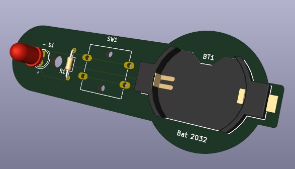
I’ve looked at SnapEDA in the past and it has been fine. I’d double check everything you’re planning on using.
For some things that are critical, size-wise, it’s a good idea to get them ahead of time and then print out a 1:1 scale of the PCB to check them against. That’s a good way to spot silly issues like using the wrong pitch or wrong row spacing etc.
Moving forward from the example PCB, I would start by allowing yourself plenty of room on the board and having things spaced out a bit for breathing room. You can always shrink it down later, it’s harder to expand things.
Keep the bottom layer for a 0V reference plane/return path as much as possible. Try to avoid long traces in it, especially when they run under traces on the top layer.
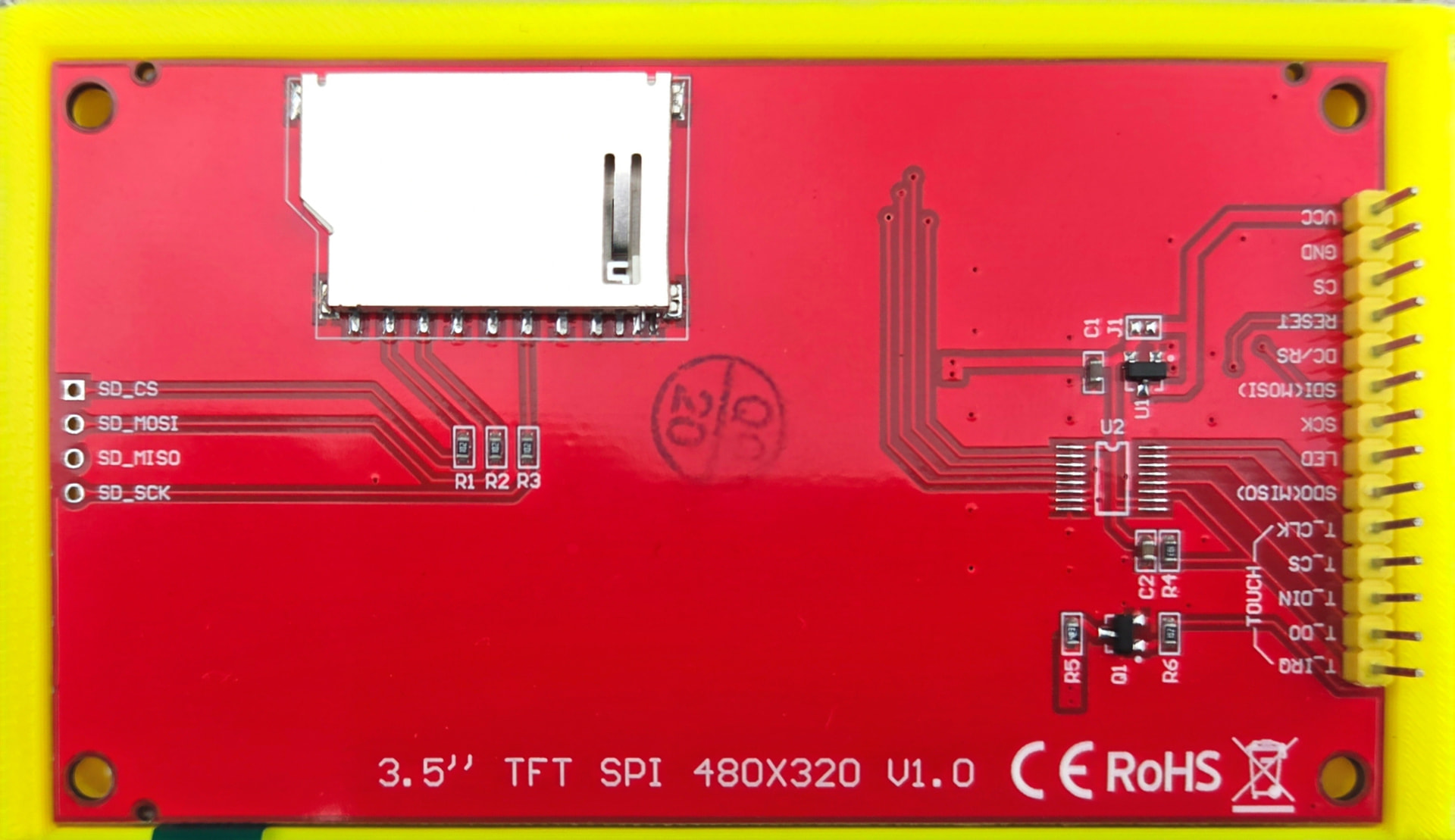
Start by trying to get everything placed in a way that makes sense. You’ll see the lines indicating which pins connect to what, spend time trying to make those make as much sense as possible. You don’t want to have 10 wires going to one thing have to cross 10 wires going to something else if they can help it. Put the effort in at this stage to move pins around, change the positions of components, rotate stuff so it makes sense, etc. Examples would be that the LCD can be rotated 180 degrees while keeping the same orientation, plugs that go off to wires can be pretty much anywhere on the edge of the board but buttons will need to be in a relatively logical location for your UI/UX consideration. Use the flexibility of things that can be flexible, for instance.
More pins is good, but I’d also say that it pays huge dividends to try to avoid feature creep as much as possible. It may feel good to try make a board that can do everything you’ll ever want to do, but you’ll pay for that in design time, complexity, troubleshooting effort and wasted money if you have to have it remade. Instead, I prefer to just make sure I can connect to any spare pins in some relatively easy way, so I can add some hand wired sections if I need to. In your case with an ESP devkit, you can easily tack wires to the solder joints for the pin headers or even add another interposer board in between yours and the ESP32, so I would be confident you can easily add stuff later without needing to design it in now.
For SMT components, I’d recommend at least 0805, potentially even 1206 if you’re not confident with SMT soldering. Having a good temperature controlled iron with a good quality tip helps. Some thin solder wick, flux paste in a syringe, thin solder and some isopropyl alcohol and swabs for cleaning up afterwards make life easy. Also a good set of tweezers, ideally ones that don’t go to a point but to a ~0.25mm flat or something. Consider how you might add some magnification, too. In an ideal world I assume you’ll get the board assembled by someone like JLC PCB and it’ll all work first try. In reality, be ready to have to replace components due to them being backwards, upside down, needing to lift legs and solder jumper wires onto things, change components values etc.
I’d also avoid anything smaller than a SOD-123, SOT-23, SOIC or similar for discrete components. Avoid no-lead packages if you can (like QFNs, CSNs, etc.). Avoid fine-pitch TQFP and TSSOP packages where possible, too. Unless you’ve worked with them before, they can be frustrating without decent tools and experience.
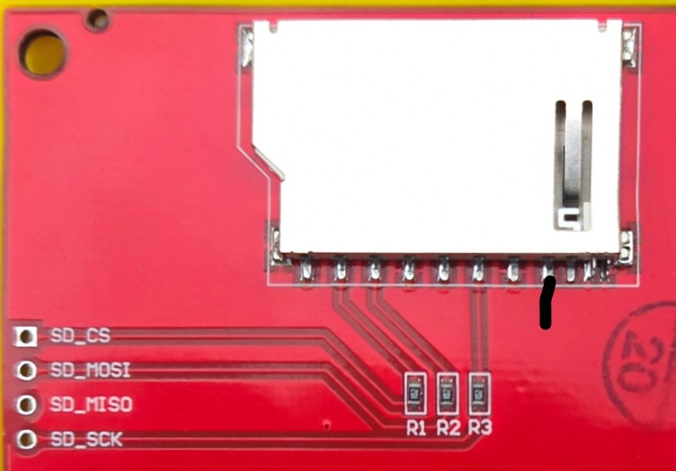
It’s also a good idea to put a series resistor in line with every single connection you make between ICs. Not only does that give you a way to route wires underneath without changing layers, it can be useful to limit current in the event of an incorrect connection and to slow down the logic transitions, which will make it less likely that they interfere with other signals on the board, etc.
Make sure every single power pin has a dedicated 100nF or 1uF decoupling capacitor, something like a 25V X7R is fine. When you do the placement, place this so that they’re close to the power pins and keep them there. Power traces should be routed into the pad of the decoupling capacitor first and then into the chip. The 0V side of the decoupling cap should be taken out sideways from the pad and go to a via to 0V as close as possible. Better is use one on either side, etc.
That’s a bunch of random thoughts to get started. If you have a read through anything I’ve written on the Jackpot posts there should be some similar PCB design related information there, too.
Glad to see someone else giving this a shot. I’m just going through the process of bringing up a 1000V/50A high frequency inverter design at work for a 20kW wireless charging system. So far it’s going well, we’ve reached 50% rated power with zero issues, so that’s fun.
 Usually we’d have pin headers on the PCB and in-line sockets on the cables.