PCB design for a ESP32 coffee Roaster board

Man, I bought my original Leaf back in 2014 when we had a demo kit that was getting installed on them for a trial we did in London. Then later I bought my model 3 when working for a different company that was using model 3s as a demo fleet. Both times I was promised a system and it never eventuated. I don’t even really have any of the charging challenges that they suit (dedicated park in a garage, easy access all around the vehicle etc.) but would still really love to have one. Alas.

The wireless charging part isn’t even all that difficult, honestly, it’s the integration into the vehicle that’s tricky.

That’s the crazy thing to me, it has always been a complete inevitability just purely on the physics of the situation and there was so much interest from all the big auto manufacturers in EVs… And then it just never really got out of the blue-sky R&D parts of the company, people developed this irrational left/right divide on the topic and here we are.

Ah nice, seems like there are some interesting things going on with some of the manufacturing changes afoot, at least!

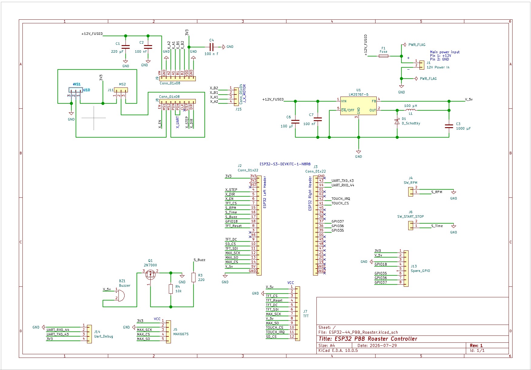
I started working on this custom board yesterday. My real ESP32 should be in today so I can start working on the prototype that matches the pins used on the custom board.

I had not thought of that use of resistors.

I am working on getting the input power section of the board done to start with, so I do not get bogged down in the details of the whole board. I was initially going to use a AP63205WU buck converter, but it is rated at 2A which is probably fine except I had the crazy idea to use a USB web camera (probably a Logitech C270) to check the color change in the coffee beans and have a standard grey scale target of some sort for lighting variations. I will test this on the prototype so will know whether it is a good idea or not before having a custom board made. If I use the USB camera it might need more current, so I am leaning to this 3A buck converter: LMR51430XDDCR Here is the datasheet on that: LMR51430 SIMPLE SWITCHER® Power Converter 4.5-V to 36-V, 3-A, Synchronous Buck Converter in a SOT-23 Package datasheet (Rev. A)

I have seen some discussion on reverse protection circuit on boards. That is one thing I have not done is accidentally swap the +/- leads. Is that something worthwhile putting on this board.

I am planning to use 12v input voltage but wondering if it is worth the trouble to design it for 12v or 24v like a lot of controller boards do.

Any SMD components I would have assembled by the manufacture, but I had not considered they would do it wrong. Based on some stuff I have received from China, I should have considered that. When doing the udemy exercise of going through the process of ordering a PCB, I see www.nextpcb.com currently has a promo for free assembly of 1-10 boards. I am not sure they will still have that when I get around to ordering a board though.

The simple switchers are great. Just pay close attention to the switching loop and keeping it tightly routed, otherwise you can create EMI issues for yourself.

I’d personally go with something like a 7805 drop in replacement buck converter like I linked above for simplicity, but I can’t remember if they go up to 3A.

It depends on your priorities but I usually would. It adds components/complexity/cost but saves you from silly mistakes. If it takes $1 and 10 minutes to add but will save you from wasting $20 and an hour on the 10% chance you do something absentminded later, I’d say it’s worth it. It’s always about tailoring the solution to the problem and there’s no one-true way of doing anything. You can implement it super cheap or make it expensive and overkill.

The simplest is a 12V or 16V TVS directly on the input which also gives you some protection against being plugged into the wrong voltage power supply and will forward bias if a wrong supply is plugged in. I’d use something like an SMCJ16A usually. That’ll work well saving you with smaller current-limited power supplies (3-4A rated) but not against all situations. For running it off a battery where the fault currents would be higher, I’d add something like a 2A schottky diode in series with the input before the TVS, I usually use an SS14 but there are tons of equivalents.

There are methods using a FET that can work well, as well. There are standalone IC solutions that can work really well be start to get expensive, etc. It’s just risk vs reward. For a one-off that I’m wiring myself, I’d keep it simple/cheap and keep up the momentum. For my designs that I make a couple k of at a time and that get wired up by technicians at the company that I sell them to? That gets a slightly more ‘robust’ set of protection components…

As with everything, you sure can and there’s no wrong answer. The key questions are why do that? What does it take to do that, time wise? How much more does it cost? Are there any downsides?

Honestly, for your first design, I’d say to keep the momentum high, keep the design as simple as possible and make sure you’re continuously making tangible progress. You’ll be way better off getting a cheap/simple controller together quickly and testing that to find out what you need next than spending months doing a kitchen-sink build that ends up needing revision anyway.

I mean this in the kindest way possible: They will get it right, 99.9% of the time. It’s YOU that will get it wrong. I guarantee it, especially if you keep adding complexity. No amount of time spent looking at it, 3rd party review etc. leads to a perfect board every time, so you have to hope for the best (no issues) but plan for the worst (replacing components, cutting/rewiring traces).

If you want to get into it and learn to replace components with a high skill ceiling, go for it!

If you don’t want to get into anything too complex but are ok with basic stuff then keep the parts you’re using large/simple and plan for a revision if you get something major wrong.

If you don’t want to do any of that, plan for a 2nd revision to get manufactured and just assume it’ll happen. Another reason to keep the design cheap/simple at first and evolve it, perhaps.

I really can’t stress this enough: MINIMUM VIABLE… Plan to add stuff later, or add it in the lightest touch way possible. If you have to make another little adapter board to add the 3rd thermocouple or airspeed sensor or add a powered USB hub to power the webcam then all of that is a better approach, especially if this is a ‘just for you’ design and not something you’re going to sell.
I already decided today that it was just getting too complex for a 1st board and took out the 2nd TMC2226, extra MAX6675, LED and limit switches. Since I have a TFT screen, I do not really need the LED.

Absolutely. If you’re making it from an ESP32 devkit, you can add wires off to other places relatively easily. If you’re doing it for yourself, it doesn’t matter if it’s a few different dev boards chained together etc.

There’s also no reason you need to design a PCB and then immediately submit it. If you get to the end and you’re not happy, start over! It’ll be 10x faster the 2nd time around and you’ve learned a lot so it’ll be better.

I think I’ve actually submitted less than half the boards I’ve designed, personally. Sometimes the ones I’ve eventually submitted for manufacture have been YEARS later. I had a mechanical keyboard design that I didn’t make for a few years and designed 3 versions of before I was happy. It still got here and I realized it didn’t really work for what I wanted it to do, lol. Same thing with a little capacitive touch macro pad. Left it for years and then finally got it made when I had a use for it. It’s surplus now but worked great for a while.

I made my 1st mistake with this project although I kind of expected this. For the breakout board on the genuine ESP32 I bought the pins do not fit. Mine is 25.4mm total width, but distance between pins is 22.86mm. I did print out the circuit board with the part I added from snapeda and that does match the footprint of my board, so not really a big deal. I do have my 38 pin esp32 prototype to play with which has enough pins for what I am currently using it for.

I also decided to simplify this design a little more and use through-hole connections and use a socket BTT standalone TMC2209 driver which I already have several of. What started this change was it seemed like the TMC2226 surface mount component wiring was starting to get too complicated for my 1st board. I was originally wanting to use the TMC2226 because it created less heat and therefore give more clearance for putting the TFT display directly on the board, but then I realized I was not going to place that directly on the board anyway because I was going to use jumper wires from it so I did not really need the low profile.

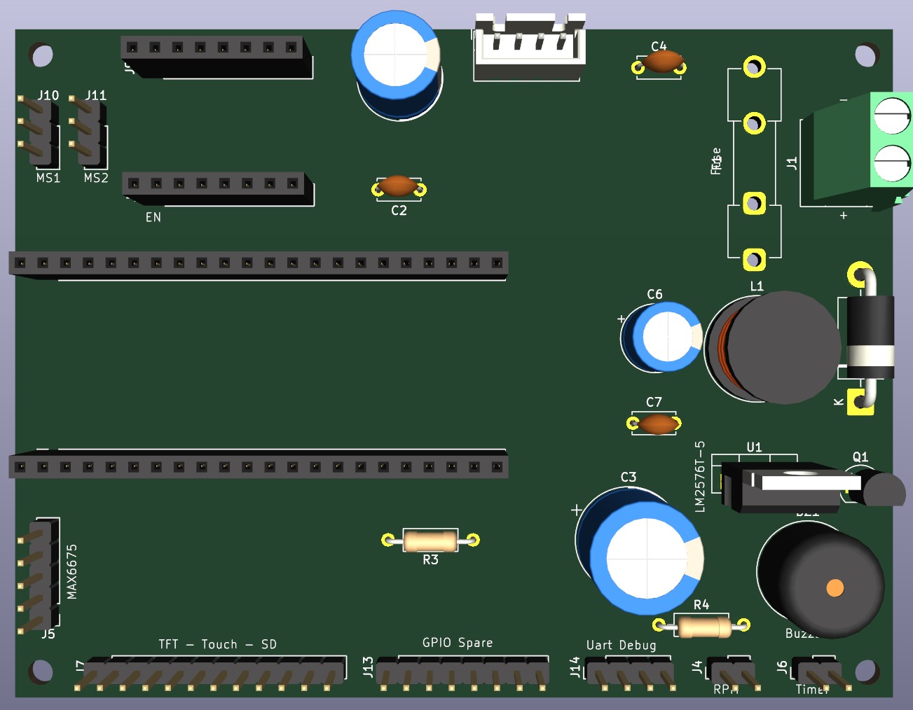
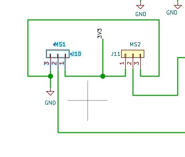
I found a couple of useful links for helping with the wiring for the TMC2209. I want to be able to set the micro stepping with jumpers for the MS1 and MS2, and this design gave me a good method for that. https://oshwlab.com/aikopras/tmc2209-driver-board and this one helped with the TMC2209 wiring. GitHub - m47812/Custom-3D-Printer-Controller: A fully custom 3D Printer controller board based on an stm32f7 controller with TMC2209 stepper drivers · GitHub I am pretty close to getting the schematic done and have been updating the PCB as I add different components but have not routed any wire on it yet because I have not really placed components very well. I have the size of the board at 120mmx80mm and probably can make it smaller.

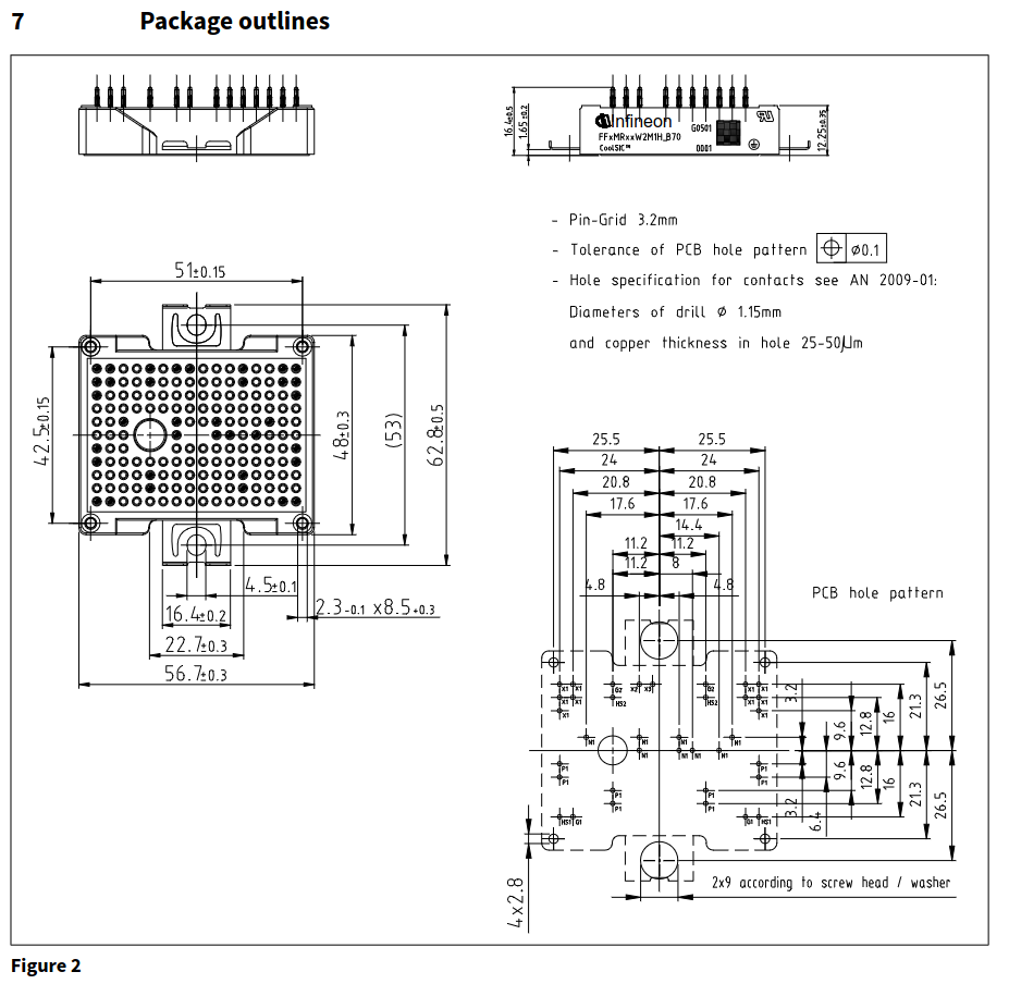
Yeah, that’s a common one, and why I recommend printing out the design and literally placing the component on it. With some extremely complex footprints and extremely expensive PCBs I’ve done almost an entire assembly into the paper PCB sitting on top of a piece of styrofoam or cardboard before. Things like this bastard:


Which costs $400 each and needs to be pressed into a 4-layer heavy copper board that costs $300 a piece to order and can’t really be re-used after being removed. You better believe that got double and triple checked by both myself and one of my colleagues before it went out. I was so, so paranoid about getting the footprint mirrored or connecting a pin to the wrong net etc.

Great idea. Simplifies things a lot and if you’re going to through-holes, it’s a lot easier to fix things like incorrect pin orders etc.

That’s a good example of where you can potentially make not-really-PCB changes that make life easier. Choosing to use wires instead of headers can make a design a lot less ‘brittle’. You can relocate stuff way more easily, rotate/flip things, etc. You can also get longer headers as well which will give you plenty more space.

Nice. Feel free to post it up here and I’ll look over it for some feedback.

Yeah, that’s a decent approach. I try to get the schematic done before even starting placement, but that’s usually because I’m designing something relatively specific and not too free-form. Nothing wrong with doing it that way and even doing some routing to test how it is, but I’d caution about getting too far ahead before finalizing stuff because often things get messy if you try to adjust them. There’s a lot to be said for doing a quick/dirty routing job just to see how it’s going to go but with the idea that you’ll completely rip it up and start again because then you know which signals are going to be difficult/annoying. Things like knowing you need to come out of an IC in a specific way to route cleanly to the microcontroller, stuff like that. You can also think of things in multiple ways, trying to route from the microcontroller out to the peripherals, trying to route from the peripherals back to the microcontroller. Routing power first, routing power last, etc. I usually try to at least start with getting power and stubs (sometimes called escapes) out from the microcontroller and other dense parts, then I’ll worry about connecting it all up later.

There’s definitely a balance with this. Obviously the larger the board the more it costs, but I’m a big fan of leaving boards larger than needed because it gives space to line components up, place/route in a way that’s understandable, keeps signals a bit more spaced out and less likely to have cross-talk, etc.

Also, I always try to make my boards a multiple of 5mm or 10mm for the outline, as well as giving at least 4 mounting holes in the corners, usually M4 and 5mm in from the edge so they’re on a predictable grid. It’s awful having some design where it’s a 118.4mm x 93.7mm board and the mounting holes are all just randomly placed so they’re not even really a rectangle. Just more things you can get wrong.

Another thing that’s quite nice and makes for a more professional touch is to plan to spend a bunch of time at the end adding notations/silkscreen to the board. Label each connector with its purpose, label each pin on the connector with its function, make notes like 9V to 18V @ 2A for the power etc. It’ll seem silly now when you’re so focused on the design but I’ve pulled boards I made over a decade ago out of a box and used them and it feels silly to have to go back and reverse engineer your own damn design…

I had that happen. Got annoyed. Then found that not all pin headers are the same diameter, and had some other ones that were a bit smaller laying around I think. I can’t remember what ESP KiCAD part I used.

I need to look at my Arduino CNC shield v3 today to see the order of the pins for the nema17 as I would like to keep that order the same as I am leaning towards using a JST connection for the motor since most of my motors have those. The planetary gear motor I am currently using does just have a DuPont connection though.

I am thinking of back peddling a little more. Since I have cut back on what I am adding, I am thinking about using a more standard 38 pin board like the Jackpot earlier version used. I was thinking that getting a real ESP32 board I would have less problems but does not seem the case. Here are the pins I am currently planning to use:

Function Suggested GPIO
X_STEP 25
X_DIR 26
X_EN 27
SPI SCK 18
SPI MOSI 23
SPI MISO 19
TFT_CS 5
TFT_DC 21
TFT_RST 22
SD_CS 13
TOUCH_CS 14
TOUCH_IRQ 34
MAX6675 No. 1 CS 32
MAX6675 No. 2 CS 33
Button 1 35
Button 2 36
Buzzer 17
TFT backlight control 16
UART TX 1
UART RX 3

With that said, what is the best target 38 pin esp32 board to use for this controller.

This is where I am so far. I might just stay with the 44 pins as it does give me some more flexibility of extra pins if I want to test something I have not thought of yet. I might add the reverse polarity and 12/24v but have not decided that yet. I have the board size down to 105mm x 80mm. I left space at end of ESP32 as it hangs over the pins about 10mm and space behind the buck convertor in case I need to add a heat sink.

If you’re supplying it from something like a 12V/2A power supply, you won’t be able to actually blow that fuse so it might be a bit unnecessary. If you’re using a battery, it’s a good idea, though.

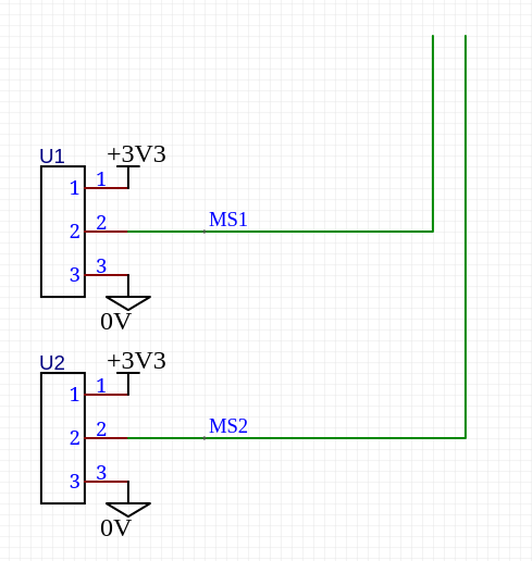
For that bit, I’d just use a 3V3 and GND net name for each pin like this:

That gets the idea across while keeping extra lines off the schematic. It also aligns things a bit better and avoids going ‘up and around’ that connector, which makes it simpler to trace with your eyes. I’d also use what EasyEDA called the NetFlag up in the wiring tools instead of a netlabel.

Adding netlabels for all the nets also helps to make it more obvious what you’re actually routing on the PCB. I try to have every net labelled unless it’s just a short stub between two components or something like that. Every net that actually heads out from a connector would be labelled, for instance.

If you’re doing it all through-hole, are you going to assemble it? If that’s the case, I wouldn’t worry too much about adding extra resistors. Normally I’d have them everywhere, like in those MS1 and MS2 lines just because it helps avoid something like the wiring being wrong from blowing stuff up, resistors in the step/dir lines help slow down edges and reduce EMI, etc. I guess the thing is, adding ~30 resistors in a SMT design that someone else is assembling is easy. Adding 30 resistors in a through-hole design that you’re doing by hand is a pain in the ass, so maybe not.

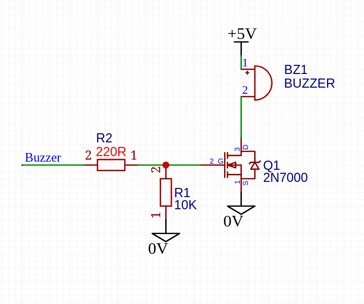
I’d rearrange the Q1 section, too, to look a little more like this:

It makes the arrangement a little more obvious. The ‘logic’ of the circuit is flowing left to right. The FET is in a ‘normal’ orientation, the pins are in roughly the right places relative to their voltages (lowest voltage at the bottom, highest towards the top etc.). The pull-down resistor is obviously a pull-down, that kinda thing. A lot of stuff like this is just convention that takes a while to get used to, but it helps A LOT. We’re really good at pattern matching, so there’s a lot of mistakes that we can spot in seconds just by looking at something and going ‘that looks weird’, before we’ve even identified what the actual issue is. Drawing something in a non-standard way means you’ve gotta trace all the connections, I had to look super closely at the FET symbol to know which side was the source, I had to look specifically at R4 and go ‘ok, 0V on one side, gate on the other, so that’s the gate pull-down…’, etc.

For the circuit around the simple switcher, I’d typically use separate net flags for each component to make it a little cleaner, but that’s just my preference. I also typically try to avoid 4-way ties like the one on the 0V connection of U1, just because that’s another of those things that make spotting errors easier. If wires cross and never connect, an accidental connection immediately jumps out as wrong, and there are definitely times when you’ll need to cross wires.

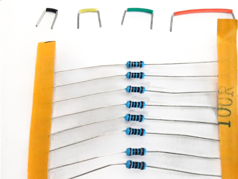
Thanks for the nice, detailed response. I will certainly use your design when I get back to working on this during the week. I was starting to think about your idea of putting 0-ohm resisters on the board to allow easier wiring on the front of the board. Instead of through hole 0-ohm resisters how about if I used these precut breadboard jumpers. I attached a photo with some real resisters for reference size. The yellow size is probably the closest match to these resister lengths and goes to between 4 breadboard holes.

I did order one of the “N16R8 KIT C” model from this listing today as I do need a good breakout board for prototyping this design. I ordered it with their ESP32 board so it should fit the breakout board if my original one does not.

https://www.aliexpress.us/item/3256808604492418.html

I also got one of these 4.0-inch capacitive touch screen with a micro-SD slot.

https://www.aliexpress.us/item/3256807312886680.html

Both 0R resistors and wire links are a common technique when using single sided board but shouldn’t be needed for most basic double sided designs, given you can go to the bottom layer to get around/under things.

Those breadboard holes will be on 2.54mm/0.1" pitch centers, so the jumpers will presumably be multiples of that.

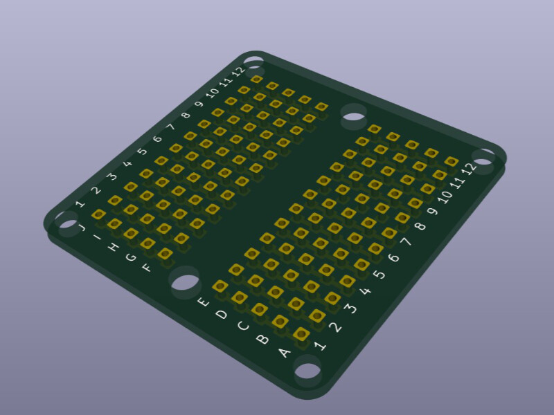
I thought these Mini PCB Prototype Boards might be useful, so I bought some and decided to play with KiCad Footprint editor and created a smaller 12 row board. I was able to create the whole board in the footprint editor. This one is 38.1x38.1mm in size. Thought I was going to use one of these boards to bring all the jumper wires from the top of the case to a central spot before jumping them to the ESP32 board but probably would be better off making a custom cable with an 8-pin DuPont connector on one end and the individual DuPont ends on the other. I need to practice my crimping skills. I do have crimp tool for these but have had limited success in the past. Here is the Amazon link for the Mini PCB board I bought. Amazon.com: ElectroCookie Mini PCB Prototype Board Solderable Breadboard for DIY Electronics, Compatible for Mini Arduino Soldering Projects, Gold-Plated (6 Pack, Multicolor) : Industrial & Scientific

Here is the one I designed and is a little smaller. It was kind of fun to design and simple. The rows of pins are tied together like breadboards.

Edit

After watching some YouTube videos on crimping including @jeffeb3 video, think I am making good progress on the crimping and they look reasonably good.

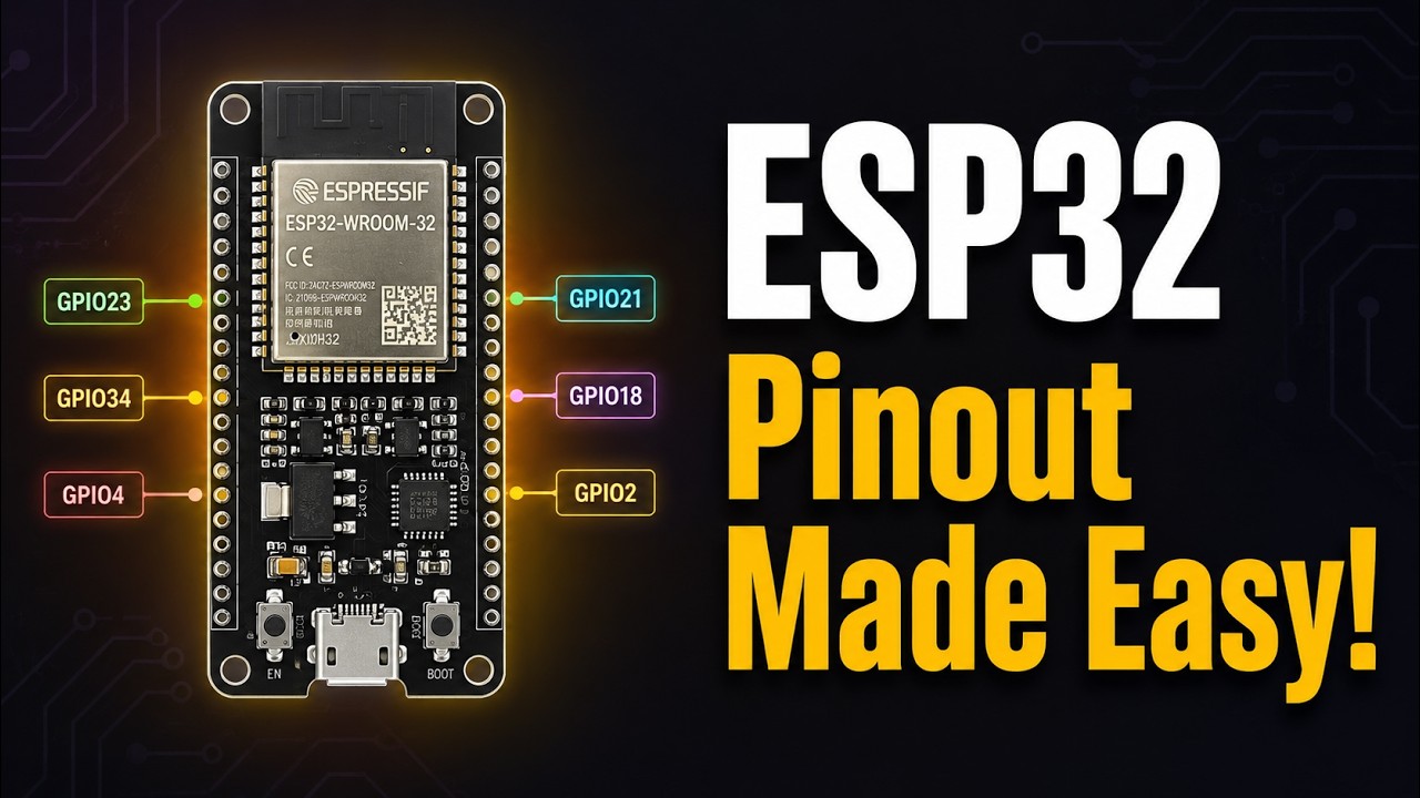
This looks like a quite useful link, an ESP Pinout Explorer for all the different ESP32 boards. Here is the YouTube video on it.

And the link to the webpage app: ESP Pinout Explorer

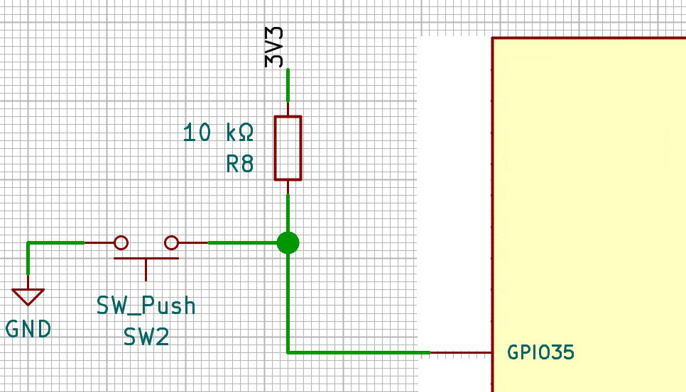
I am adding a real time clock to my prototype as I did not want to mess with Wi-Fi for Date/time. I was out of pins on this 38-pin board, and I needed 2 GPIO pins for the RTC, so I had to move the 2 buttons to read only pins. I wired a pull up 10k resistor for each button like this and it does work. For the buttons I am using GPIO34 and GPIO35. My newer board that the custom PCB is designed around does not seem to have any read only pins, so I won’t need this pull-up resistor on the custom board.

I used this YouTube video as verification to how to wire this up as I did not trust ChatGPT.

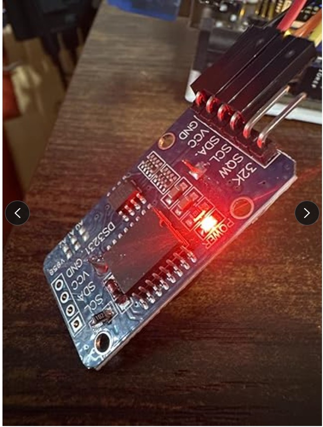
This DS3231I bought from: Amazon.com: 2PCS DS3231 AT24C32 IIC RTC Module Clock Timer Memory Module Beats Replace DS1307 I2C RTC Board with Male to Female Jumper Wire Cable : Industrial & Scientific also seems to have a charging circuit, but since it has a non-chargeable CR2032 battery looks like I need to disable that by pulling up the resistor as shown by one of the reviewers of that part in attached photo. Does this look correct?

The schematic posted doesn’t match the board so it’s tough to tell. There shouldn’t be anything connected from Vcc to the battery. From looking carefully at the pic that person posted, it does appear that there’s a trace going from Vcc to the 1K resistor, to a diode and then to the + terminal of the battery, which is quite the fire hazard…

In a ‘proper’ DS3231, it should draw basically nothing from the battery while it’s supplied via Vcc and cannot back-feed into the battery as a safety consideration.

There’s zero chance this is a proper DS3231, though, and who knows what’s going on. Maybe there’s a ton of leakage on that pin so they’ve added the external resistor to supply that, or maybe the chip doesn’t do Vcc supply properly so they’re doing this as a hack way of supplying from both.

That board design is also utter garbage, but oh well.

I’d lift it or just clip it off the board with pliers, personally.

If you’re running short of pins, you could always try find a DS2417 on an eval board like that and use the 1-wire interface. Or, if you’re using I2C, move something else to an I2C interface as well…

The schematic was a screen clip from the ESP32 that I am using on the custom board which does not match the board I am using with the Read only button which is probably what you meant by not matching the board. I should have just had GPIO35 listed and not part of the outline.

I tried to just raise one end of the resistor but ended up just pulling the whole resistor off and it went flying in the shed somewhere. That is the 1st time for me desoldering a surface mount component and did accomplish the same thing. After desoldering, I put the battery back in and reset the time. I will check the time on it in the morning to see if it is still correct.

The schematic from the Amazon link.

Yeah, it’s not really a good idea to try to lever the resistors up like that. You really need to have both joints flowing to remove a component. My preferred approach as a simpler option is to put a bit of extra solder on both ends and then use a larger iron tip to try heat both at the same time. Alternatively, you can try to wick all the solder off one side and lever it up a little, but any kind of mechanical stress on the component can end up ripping off pads and damaging the board. In this case if you know it doesn’t need to get put back then it’s not like board damage is an issue…

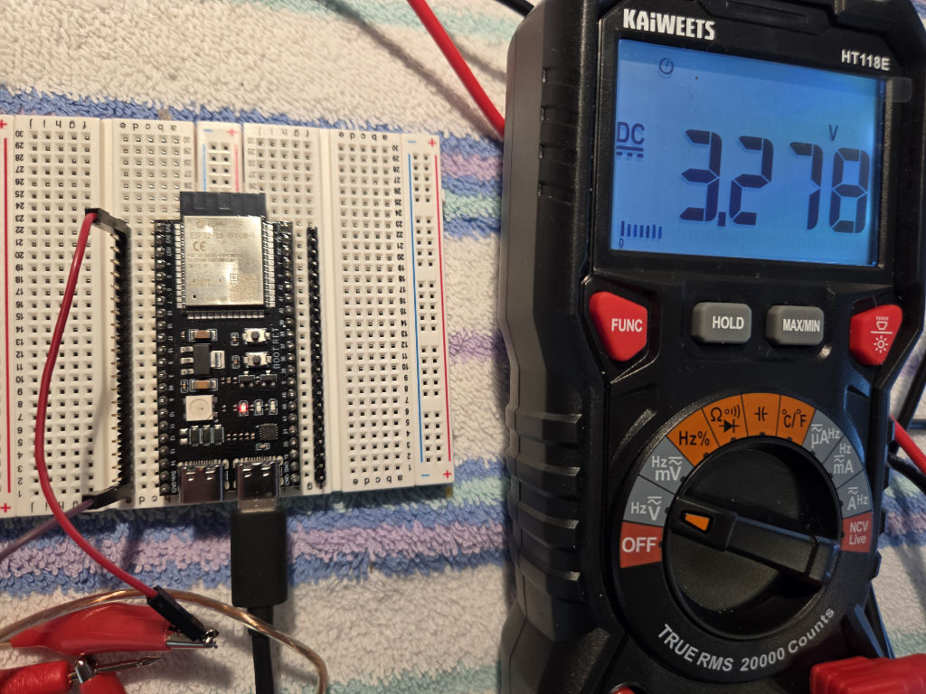
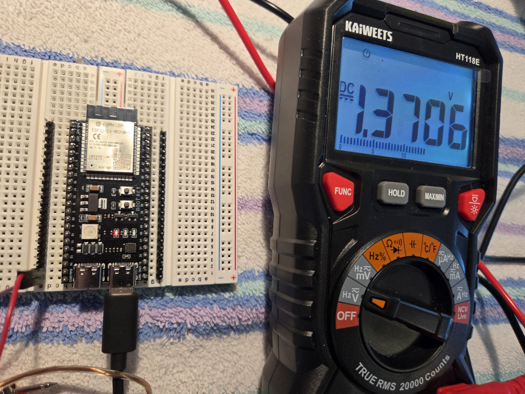
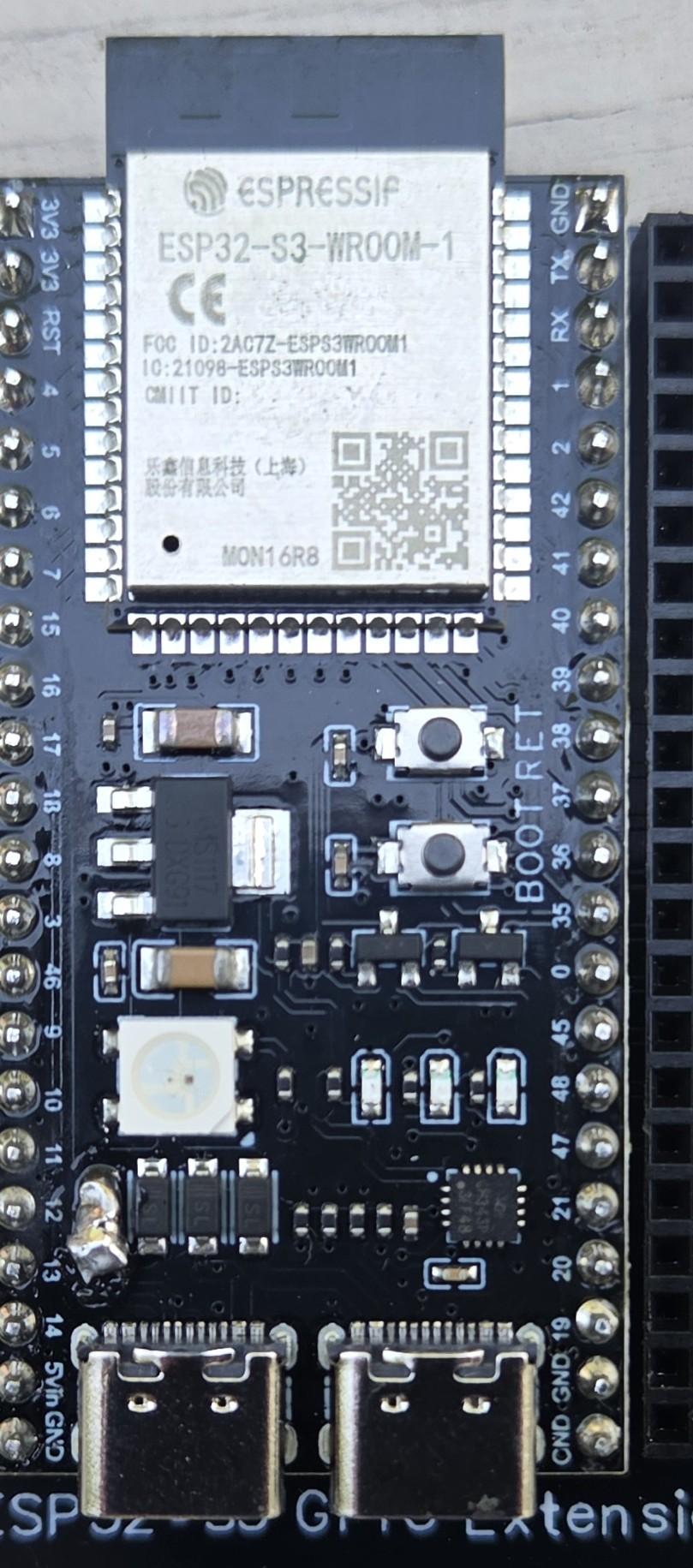
I got the 44 pin ESP-S3 clone with breakout board. I got the clone with it since I suspected my real ESP32 board would not fit and I was correct. The big problem I had with this new clone board was it measured 1.37v on the 5v line and 3.3v on the 4 pins on the breakout board that are supposed to be 5v. After contacting seller, he said those boards don’t support 5v output. He said I had to bridge 2 solder joints to get 5v. Now why didn’t they just do that to begin with since it is clearly marked as 5v on that pin. My soldering on that small a spot is not pretty but it did work and I now read 4.7v on all the pins labeled 5v. I also got the same voltage no matter which USB port on the chip I used.

The shield apparently got dented in shipping but does seem to work ok.

And here is my ugly soldering bridge work. Think I have a smaller soldering iron tip, but could not find it today.