Okay, thank you. Best to just add a few gpio breakouts.
If this works, that is easy. If not, it seems like using the expansion header is the other way since there are no components on those pins.
Okay, thank you. Best to just add a few gpio breakouts.
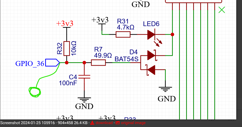
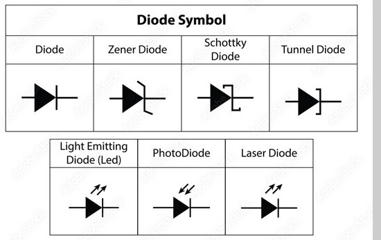
Those are zener diodes… Where is @jono035?
I’m intro college EE class circuits level. I got an A, but that was years ago, so I understand the basic circuits, but the circuit protections and inductance for smoothing and stuff like that is not something I am familiar with.
Here’s what I see from your schematic (I’d love to learn this better):
3.3V to 10K is a pullup resistor (right next to your green line). A pullup is more often to hold a line high like for a button when you short it to ground when you press it. This is considered digital IO, not an analog input. I could be misunderstanding.
This is how they do it on the octopus board:
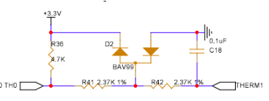
those are std diodes, not zeners because the lines by the arrows are flat not curved. Power is 3.3.V, Resistor (R36), sensor (TH0 is the board pin attachment point) , and the other end connects to ground. THERM1 is the board connection pin. I would use R36 of 50 kΩ (like the 49.9 kΩ in your example), but I don’t know the purpose of the rest of this circuit with the matched 2.37 kΩ resistors and the diodes.
I am not sure the significance of that? I am like 3rd grade level EE, not even high school.
Okay revision.
The Jackpot
-Vmot outs, handle two fans (print and extruder)
-5V out handle two SSR’s - bed and hot end
-7 inputs - touch probe, X endstop, Y endstop, 4 spare inputs.
-expansion port gives us 4 naked GPIO, that would be a touch probe pwm out, and two therms in with a spare GPIO
That is the part I was missing. I knew we were separating it I just could not remember how. That turns any input to on or off, no in between. We almost used an optical separation, that is the same thing just more robust in this case.
Easy enough. Looks like we need a simple expansion card or find room on the adapter.
Apparently I’ve been summoned ![]() That’s quite amusing, I like it.
That’s quite amusing, I like it.
@orob The symbol in Ryan’s schematic is a schottky diode. These are basically still just regular diodes except that they form the semiconductor slightly differently so it has lower forward voltage (less voltage ‘drop’ while conducting) and can switch faster, usually at the expense of having lower reverse voltage.
A zener would typically have angled lines coming off it. I’ve seldom seen them drawn with straight lines but plenty of the example images I looked up show them like that, so maybe it’s more common than I think.
The Pico has 3xADC so I will pop two out of the top of the adapter (terms), and one to the expansion header for future toys. the other Expansion pins will be regular.
Best of everything?
You just let us know if you get tired of that. It can go both ways.
I definitely will. No issues for me at the moment and I’ll be sure to speak up if I don’t appreciate being included in any specific topics etc. Even if there’s anything interesting hardware-wise going on, I usually fall off threads that spend too much time on firmware configuration etc. I’m not familiar enough with it and I’ve just never been one for software/firmware development. I’ve done a lot of it, but it’s always a means to an end so I avoid it in my spare time. It’s like painting things or sanding. I’ll do it if needed but if someone asks for help writing firmware or sanding their deck then I’ve suddenly got other plans…
I’ll take a look through the rest of the thread and see if there’s anything to add.
Have you thought about asking questions on the Klipper discord channel?
Do they need to be exactly overlaid? If only one will ever be fitted, they can also be offset slightly. Moving the pico a few mm to either side would still work. If you do go with that footprint, definitely try to keep some solder mask between the through-holes and the SMT pads. Solder paste can bridge from the surface mount pads to the through-holes (called scavenging) during reflow and castellated joints like that are really sensitive to paste quantity.
I’m not entirely sure what you mean here, but to read a thermistor you’ll only need a pull-up that’s a similar value to the thermistor and then route that to an ADC. Adding/keeping the diode arrays for high/negative voltage bypassing and a capacitor for filtering is always a good idea too, of course.
Never mind, I see the schematic in the next comment. This won’t work particularly well with the LED in place because the current through the thermistor will vary a lot with voltage, which is what you’re measuring. You could still do this and characterize it so it was right-ish, but it’s a lot more work than is necessary. Edit: Actually no, I don’t think you could. You’d be relying on all sorts of weird stuff like the leakage/bias current into the analog pin. Not a good idea at all…
What design is that from? It’s a little weird having that diode in-line like that. That looks like something is miswired, to me, or that it’s a very odd way of doing a 5V to 3.3V level conversion on the output, perhaps.
The diagram that @orob has there is much more like how it would normally be drawn, with the diode array bypassing to +/gnd as a form of protection. Basically clamping the signal when it exceeds 3.3V+Vf or 0V-Vf… Otherwise not affecting it.
We need to plug it into the esp header on the jackpot. If we offset it we will need to buy the pico with headers and add a two sided assembly to the new adapter. That is a lot of extra cost.
The jackpot, I think that was just voltage protection. I opted not to do optical isolation, so he set it up that way instead.
Hmmm, maybe we need to change it in the next revision?
If I make the pico and the headers on the same side it is cheaper to assemble, the downside is heat. But I do not feel like we will ever really be pushing it to it’s limits and really heating it up.
Before I run all the lines, does anyone have any major issues with the pico under the adapter?
Honestly it would not be a huge issue to switch it if it did have any heat issues it would just be a pin remap in config.
Not yet. I still feel like I have no idea about that side yet. I need to have it running on something before I can really get it.
So this is intended as a adapter to put a Pico in an ESP32 footprint? That’s what I was missing, my bad. This could also be done with SMT pin headers on one side and the pico on the other, obviously with the trade-off of double sided assembly. The SMT pins are pretty easy to solder as SMT parts go, though, so with oversized pads and a part chosen that has alignment pins then it’d be fine for hand soldering.
I don’t recall seeing that at all. Is that something that has changed or did I just miss it? It’s a little bit of an odd circuit so I’d be interested to know what the goal is there.
If you keep a decent amount of copper everywhere then there will be at least some heatsinking through the board and through to the top. Depending on what else needs to be on there, if you can keep the top side clear of components, a few stick-on heat sinks would likely improve the situation on the rare chance that it does get a bit too hot.
Thanks @jono035 ! that is what I was unclear on. Clamping makes it so I can’t overshoot the limits of the input in either direction. Wish I had that on the endstop pins…
Yeah, that’s the one. It’s extremely common as a method for protecting against incorrect connections (reverse voltage or over-voltage applied) but also ESD. Because an ESD strike has a lot of voltage but not much energy, if you can direct it into the voltage rail then a small ESD strike doesn’t usually cause any issues.
The alternative is to use a zener diode or a TVS, which is basically just big zener diode anyway. The downside with those is that they start to ‘leak’ current before they start conducting fully so you need to choose one with a much higher reverse voltage than you’re using or it will start to affect the circuit. They also have a lot of capacitance so can slow down high speed signals or cause other unwanted effects. Their capacitance also changes with applied voltage so for analog signals you can end up with a filter that changes frequency response as the voltage on the pin changes, which isn’t ideal.
this information is gold. I had a design with a TVS on it and I had to pick a new one and other than a simple reference circuit, could not find how to best use it with my limited exposure to that component. It ended up working and protected against reverse power connection. I was not aware of the leak tradeoff or the increased capacitance. The circuit in question was a low tech DC setup, so no issue with signal attenuation. Your explanations are very helpful.
That was always there. I think he pulled it off of one of his expansion modules. Just trying to protect the input pins. (Honesty it is not all that important because I do not place the 5V rail). Usually I think it is to protect feeding 5V into the gpio.
Any input on “protecting” the input pins? If we can do it another way and get the functionality back of all those IO that would be awesome!
Yeah, that’s a nice easy scenario for a TVS. Most of them are specified with a specific reverse working voltage which is where they’re guaranteed to leak less than a certain current (I think 1uA or 10uA from memory, depending on voltage range). The trade-off is that the clamping voltage will then be much higher, something like 30-35V for a TVS intended for 24V use.
Using a Zener in the same scenario can be a bit fraught because they really work best when they’re constantly conducting in reverse. A 3.3V Zener might start conducting slightly as low as 2V and by the time it’s at 3V it might be conducting 1mA or more. That makes them really awkward to use for protection, specifically.
pull R32 (10 kΩ) off and put the thermistor in its place?