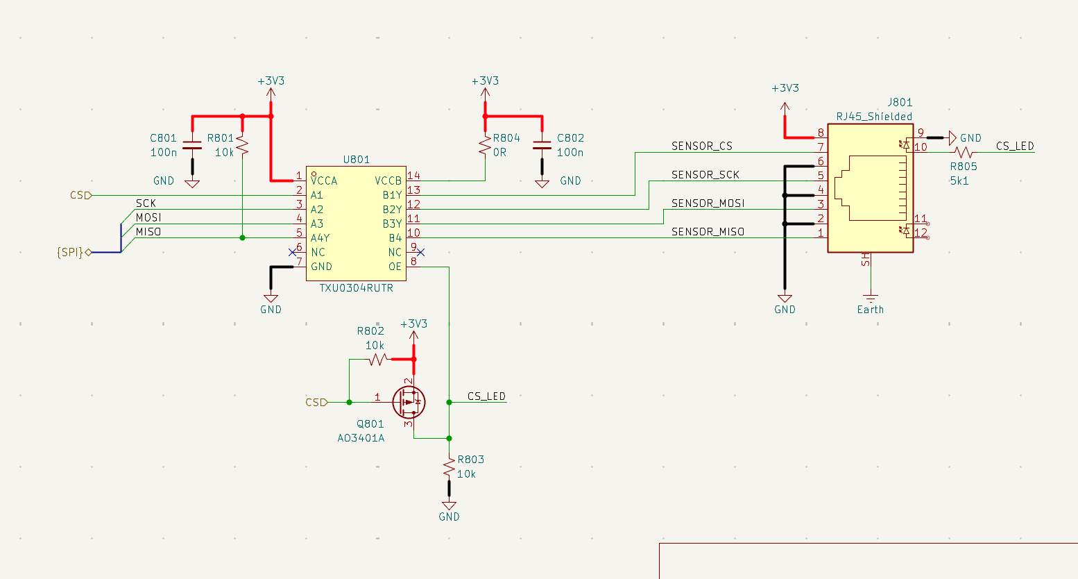
It’s splitting the lines into individual sections, each driven by their own buffer.
So rather than having say 300pF of capacitance on 3x paralleled SPI lines, you’ve now got 3x separate lines with 100pF each. The key there is that each buffer is now driving 1/3 the capacitance. How much this benefit this provides can vary quite significantly depending on the issues you’re trying to address.
If the buffers have negligible output impedance then it would have no benefit, the outcome would be the same. A 0V to 3.3V transition would have a nice fast edge rate because the buffer has enough output current to quickly charge the 300pF of capacitance. The cross-talk would be the same because the current impulse from the high speed edge on the neighbouring line through the capacitance would propagate down the line and into the driver without much voltage change due to the impedance, etc.
If the buffers were high impedance the improvement could be up to a factor of 3. Each buffer is now driving 100pF instead of 300pF so that’s 3x the high frequency impedance so 1/3 the current output requirement for the same edge rate, which means a faster transition from 0V to 3.3V with the same output impedance. Same thing with cross-talk, 1/3 as much cross-talk current means 1/3 the voltage disturbance as the driver sinks/sources that current. That’s a fair bit of an over-simplification, but hopefully it gets the idea across.
In reality it’ll likely be somewhere between those two situations. It won’t be a perfect threefold improvement in edge rates and cross-talk, but it’ll definitely be better. The downside, of course, being extra complexity, cost, board space, power consumption etc. as well as sometimes simply being not really possible without kludges that may make other things worse. That’s common with buses like SPI where you have to be able to have things like the slave device drivers go into high-Z output so that other devices are able to communicate. The network then needs a way to either know that the end device is in high-Z state and to do the same to the master-end buffer, or it needs a defined ‘idle’ state that can overridden by other devices, etc. It’s even worse again with stuff like I2C where you’ve got something multidrop with a high-Z idle state and low-Z active state. Then each buffer needs to be able to replicate that high-Z/low-Z state across it which can cause all sorts of issues. There are chips that do it but in my experience they haven a strong chance of introducing other problems/variabilities that can be remarkably difficult to diagnose.
Another way it helps is reflections, although that’s probably getting into a longer line/higher frequency consideration than your SPI links may need. As frequencies increase your wires start to behave as transmission lines, which basically just means that rather than thinking of it as a single inductor and single capacitor, it now looks like a string of tiny inductors and capacitors all connected together to make a series of LC ‘filters’. Once you get to this point, the high frequency components that make up your edge take time to propagate down the line because the voltage impulse at the start takes time to build current in the ‘first’ L, which then takes time to build voltage in the ‘first’ C, etc. all the way to the end. The energy that has been ‘waterfalling’ its way down the cable gets to the end of the cable and (in simple terms for an unmatched system) doesn’t have anywhere to go so the ‘final’ capacitor charges more than you expect and that energy then starts to flow backwards back to the start where it will look like a voltage spike when it arrives back at the driver, etc. With 3 lines all connected together, these pulses flow down one line then bounce back along the other lines, then return etc. They can be strong enough that they can cause the receiver to read an incorrect voltage in some cases, causing data corruption, or even damage to electronics in truly extreme cases. Separating the lines with buffers like this allows all of the pulses flowing around to be simpler and lower total energy, because you’ve got 1 reflection instead of 3, for instance. The other way to handle this is to have the transmission lines ‘matched’ by a terminator, which means that the impedance of the receiver is designed to be the same as the impedance of the transmission line, which means that when the energy impulse arrives at the receiver it all gets dissipated in the resistance of the terminator. Even if it’s not perfect, it’ll still usually be much better than nothing at all. That’s why with things connected by coax you’ll often see a standalone resistor to return near any receivers or transceivers. Same thing with ethernet or high speed differential signals. For stuff like DDR interfaces it starts to get even gnarlier, but that’s a bunch of steps beyond this again.