Well had to try and figure out how they work, what better way then to replicate it?
See any issues?
They come out to about $7.50 in bulk before taxes and import fees.
Well had to try and figure out how they work, what better way then to replicate it?
See any issues?
They come out to about $7.50 in bulk before taxes and import fees.
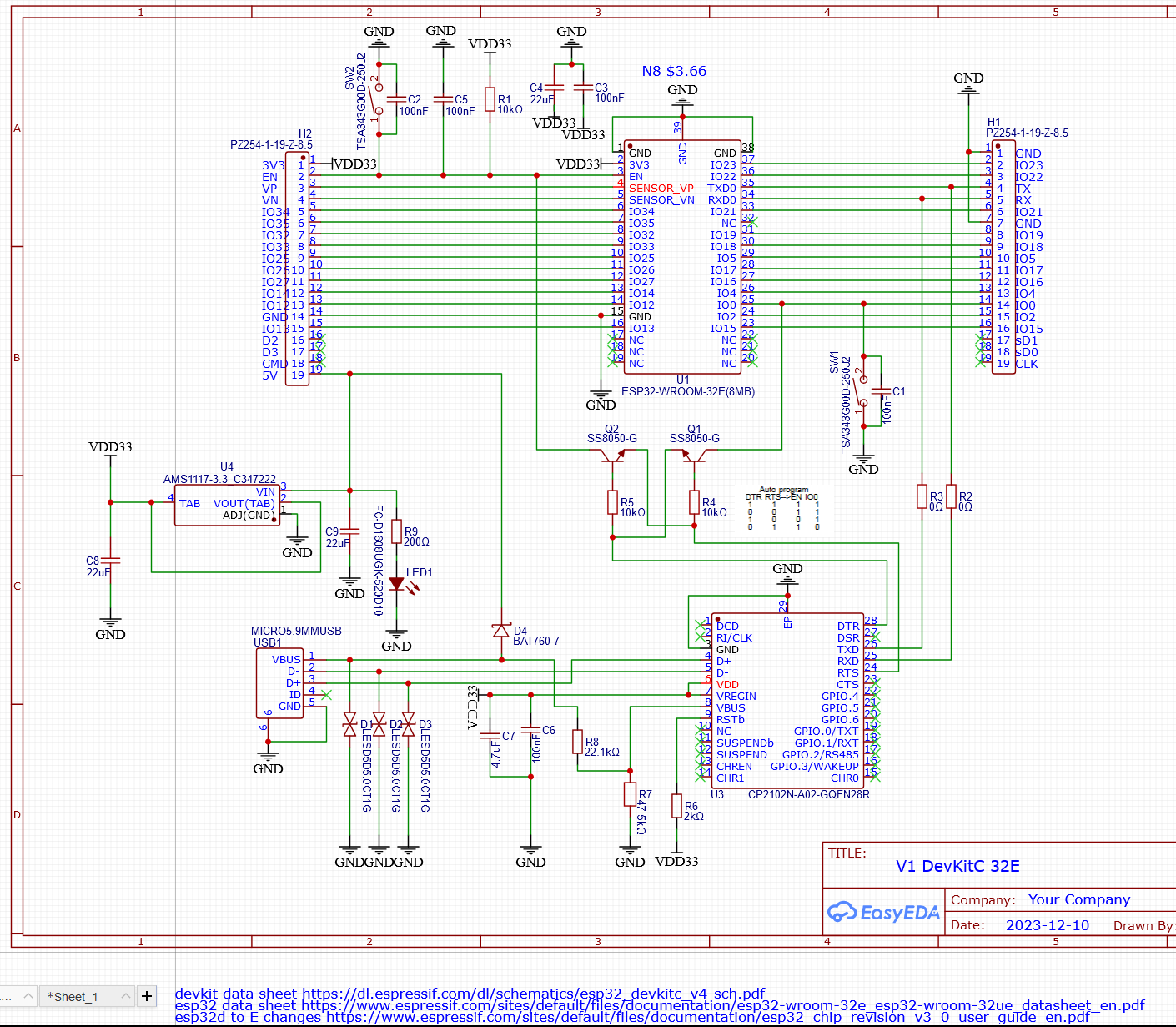
devkit data sheet https://dl.espressif.com/dl/schematics/esp32_devkitc_v4-sch.pdf
esp32 data sheet https://www.espressif.com/sites/default/files/documentation/esp32-wroom-32e_esp32-wroom-32ue_datasheet_en.pdf
cp2102 usb- https://datasheet.lcsc.com/lcsc/2304140030_SILICON-LABS-CP2102N-A02-GQFN28R_C964632.pdf
I went through all the trouble, if these look okay I will be buying some. Just to get the V1 graphics and maybe some cool colors. (and to prove it works)
The only chip that needed special attention is the USB chip and it wanted the two caps as close to the power in as possible.
I can add a few more grounding vias, and some V1 graphics but I think it is functional at this point.
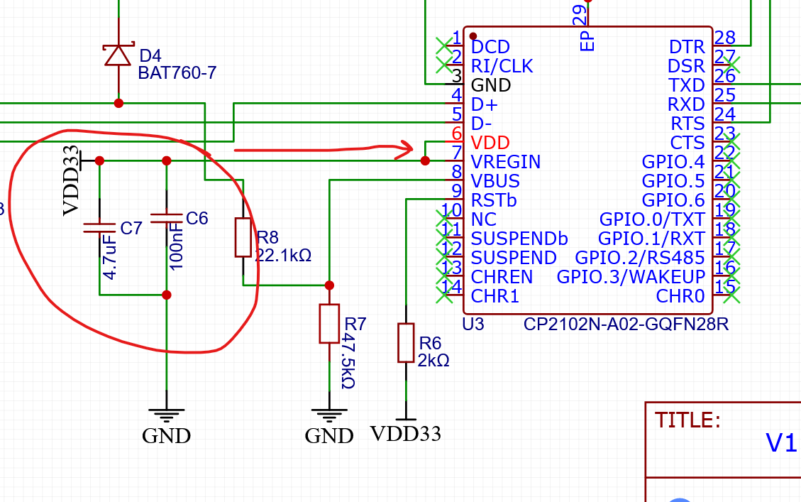
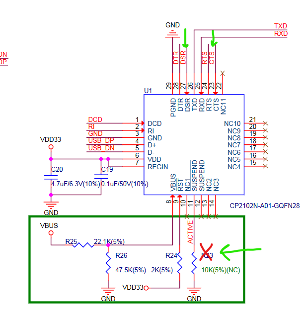
I did not add R23 it says (NC), Not sure why that section is in a green box?
DSR, and CTS have no connections, so I assume they are not needed? You can see the few pins I have used above.
For future expansion: add uart port and pins, given the plans of fluidnc team to add uart based io extender (for instance for pendant etc)
? That is already in the jackpot board. The ESP32 Devkit has all usable pins broken out already.
I thought you were going to add the esp32 to the board, soldered, but it looks like you are just making your own dev kit?
sorry, wasnt clear enough, on a new board it might be worth it to add a seperate/dedicated header for this future expansion purpose
It is already there on the Jackpot. A whole separate headed with modules already available.
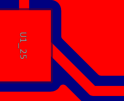
Devkit first. I doubt I will ever combine them but if I did, this is the first step to make sure I did it right.
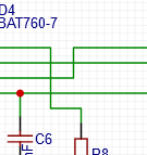
When you put the caps as close as possible to the VIN, I would say C6 (lower value, higher frequency) should be closer than C7, all else being equal.
According to the datasheet, suspend and /suspend on the CP2102 are digital outputs indicating USB suspend status (whatever that is?). So I think it is safe to leave it floating if you are not using the output.
Thanks I will swap them right now.
Cool! I read through it a few times and really had no clue if that was a standard thing or an extra thing.
Planning on having Pcbway, JLCPcb or someone else fab and assemble?
Curious how much it’d cost for them to also upload firmware, and basic test 2nd or later batches of boards. Ideally, eventually, they’d be provided with couple of test boards that verify functionality, so kits are QA’d before you even receive them.
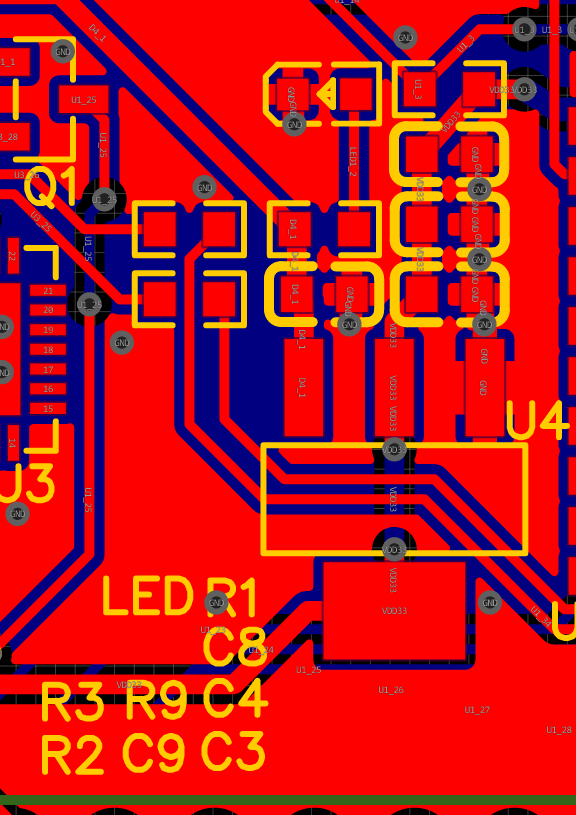
I always try to keep rails/grounds such that a wire goes ‘down’ to the ground port and ‘up’ to the voltage port. This makes it easier to see at a glance whether something is correctly connected and whether it’s pulled up or down. I would also try to avoid 4-way crosses like with C9, R9, U4-3 and the net up to H2-19. In this case it doesn’t matter, but it’s better to be unambiguous about whether 2 wires should be connected.
With something like the D-/D+ routing, I’d probably just do that with netlabels. There’s no useful information added to the schematic by having them wired out and the crossover is harder to inspect for correct connections than just looking at the netlabels and going ‘yeah, D- goes to D-, D+ goes to D+’. In fact, in most of this schematic I’d go through and try to think about whether a connection is better done with wires vs netlabels.
Wires are good because you can easily follow everything that connects to them. For a design this simple, that’s not too much of an issue. Netlabels are good because they’re typically easier to inspect by eye and leave the schematic much cleaner and simpler looking, which helps with being able to inspect stuff that can’t be done with netlabels. I think the devkit schematic kinda goes a little bit too far in the other direction by using netlabels for damn near everything, though. I typically aim for a mix and using whichever one where it makes sense.
Honestly, I’d probably ditch the AMS1117-3.3 in favour of a different part from a western manufacturer, assuming JLC have them in stock. Typically I end up a generic equivalent of a TI part like a UA78M33CDCY. I’ve had more than a few of them die when being used within their ratings, although that’s less likely to be an issue if the devkit is being powered by 5V in the Jackpot. I can’t actually remember whether it is or not, though.
Probably too late to do much about it now, but typically I’d use different ESD suppressors on Vbus vs the data lines with the USB input. Having something larger like an SMA TVS on VBus gives you more protection against things like actual surge events, rather than just ESD.
As Jamie says, swap C7 and C6 positions.
I suspect C2/C5 are redundant so I’d only fit one of those. That looks like a mistake on the Devkit schematic, to me. I’m also not really a huge fan of putting a capacitor across a tact switch like that to debounce it, it causes arcing on press and can cause them to eventually weld closed or fail. At the very least, I’d normally put a low value resistor in line with the switch switch, something like 100R or so. In this case, if the goal is to just recreate the devkit then I wouldn’t worry because the buttons are likely to only be pushed maybe 10-20x ever, but it’s a kinda crappy thing.
R9, the resistor driving the LED is 2kR on the devkit and 200R in your design. That’s ~17mA. I can’t see the specs on the LED, but that’s a lot of current and brightness for an always-on power indicator. If R9 is 1/16W, you’re also a little close to its power rating. I also can’t tell the colour, but it looks like you’ve gone for a green LED instead of red, assuming that’s deliberate?
They do flying fingers but I don’t think anything else is offered.
Understood, In this case it is definitely not clear.
I laid it all out so I could SEE how it is all connected. I understand the schematic but SEEING it really helped me here.
I don’t know enough to swap components that easily. I will look around, though. Same with the cp2102, we use hardly any of it, I am sure there is a comparable part better suited.
What might I look into? I just followed the espressif docs. I know next to nothing about EE stuff.
Swapped already. Is there a chemical difference or just the size? How do you guys know which is faster?
Awesome.
I looked at some online calcs for the value. I put in a resistor on the lowest/dimmest end of the chart on the spec sheet. I was a little worried it would be too dim. Yes Green, hopefully same color as the board ones.
For the layout:
For the linear regulator, U4, you REALLY need that tab to be connected to a decent chunk of copper as that’s where the majority of its cooling is coming from. I always prefer to use devices that have that tab be grounded where possible which makes layout way easier, but if I can’t avoid it then I’ll move it somewhere away from everything else and give it its own chunk of plane that’s connected. How much plane you need depends a lot on how much power its dissipating, but I’d typically aim for at least a square inch. The datasheet will have specs for the expected thermal impedance when attached to a plane of a specific size. From the AMC1117 datasheet, it looks like the bare device has a junction-ambient of 136°C/W. Assuming 40°C ambient, 150°C maximum junction temperature, that gives 90°C worst case before shutdown. Add a bit of safety margin and say 70°C. That means you’ve got around 0.5W of power handling. With 5.5V into the regulator and 3.3V out, that’s around 200mA max. That might be enough, but it’s all cutting it a little close, in my opinion. In comparison, the device has a junction-tab of 15°C/W and a PCB heat-sink of 500mm² has 59°C/W so if it was connected to a 25mm x 25mm pad, it has a total junction-ambient of 74°C/W, which is closer to 1W of power handling. Honestly, I’d probably swap this out for a better linear regulator that has a grounded tab. Having the tab be on the input/output really does make life more irritating than it needs to be. I suspect that’s because it’s fundamentally an adjustable regulator that is likely just configured with internal resistors or laser-trimmed to be 3.3V, rather than a dedicated part.
I’m a little concerned at how close D1, D2 and D3 are together. At the very least, having silkscreen over pads isn’t good. I’d rotated D2 90 degrees so that the ground is ‘up’ and move the entire thing right a little.
The thermal relief on all of these parts is unbelievably ugly, I’m not sure why it’s doing that. I would significantly reduce the width of the thermal relief spokes. You’ve also got vias crowding your thermal reliefs in a bunch of spots that are starting to look a little ugly, too. I’d move them further away.
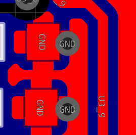
GND on D3 for instance:
The return path for this ESD diode is into the connector ground, so it’s not actually all that critical to have the via right there I’d move it out so it isn’t in the gap around the thermal relief. That’s also a good example of where thermal relief isn’t being treated properly.
GND on C1:
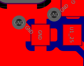
Don’t route grounds if you’re using a pour. I can see there’s a trace under there that’s also interfering with the thermal relief, although not terribly.
C1 and C2 also have their designator on top of the pads.
D4 designator: This is just a personal preference thing but I like to keep the designators in the same ‘orientation’ as the part, if I can. It gives a little extra clue which part it refers to, in case it can get ambiguous. In this case, rotating the D4 designator by 90 degrees makes it match the shape of the body of the part, similar to how R4 and R5 match. I’d also do the same with Q1 and Q2 but it’s less important as they’re more obvious.
I also try to keep at least 0.1mm, ideally 0.2mm between any silkscreen, otherwise it all bleeds in. It’s not a printing process onto a medium like paper where it soaks in, instead it’s closer to marking with a layer of paint that stays on the top. The space between lines is as important as the line thickness to avoid them bleeding together with surface tension and becoming unreadable. Think of it like milling something out, the thickness of your end mill is important, but so is the thickness of any remaining stock. You can’t cut a pair of 3mm wide slots side by side and expect them to leave a 0.5mm thick sliver of stock there without it failing.
For situations where that gets awkward like the block of passives above U4, I often move all the designators somewhere else and just arrange them in the same ‘shape’ as the organisation above. Something like this:
Personal preference, but I’d try to make entries like this one into the top of the BOOT switch 90 degrees or 45 degrees into the corner of the pad. That’s an ‘old school’ requirement due to the potential of trapping etching acid in the acute corner of the trace and over-etching it, but there have been a few people that have ‘proved’ that this isn’t an issue anymore. Regardless, I still think it’s good practice:
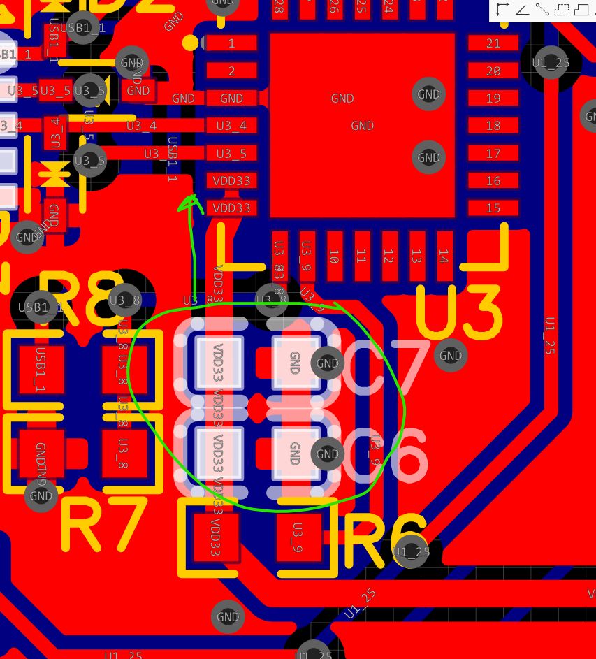
C6 and C7:
A via in between these two would be a better, lower inductance position, but if that doesn’t work then I’d still probably try to move them to the right so they’re not interfering with the space around the thermal relief.
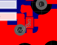
U3 pins 6 and 7:
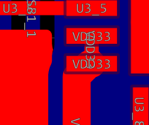
I would avoid having traces jump directly between pads like this where possible. It can result in solder scavenging from one pin to the other, leaving one dry and not connected. I’d also neck the trace down so that it’s not a single huge wide trace going into the chip. Having a 0.5mm long section of 0.2mm instead of 0.5mm is never going to be enough of a difference to affect anything. Hell, all your power traces can be routed in 0.2mm without issue here. If you take a look at the Saturn PCB Toolkit, 0.2mm wide trace is good for an amp and will see 8mV of drop at 100mA over 30mm. I always like to route the power traces larger where it doesn’t hurt anything, but in this case the more important thing in the ‘hierarchy of needs’ is making sure that the layout is clean from a board assembly/reliability standpoint. I’d go to 0.25mm or whatever the pad dimension is, come into both pads from the left and then route down the outside from there.
I’d also have tried to put C6 here:
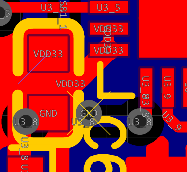
With the GND via there. That cap is the one that’s providing the high frequency decoupling into the chip, so getting it as close as possible is a good idea. C7 is handling the lower frequency/closer to DC stuff so it can be damn near anywhere without issue.
I see there aren’t any really any stitching vias yet from top to bottom. I’d add a few around, ideally making sure each is within 10-20mm of each other. I’d also add a couple on each side of VDD33
where it’s on the bottom layer under the ESP32.
A bunch of the vias under the ESP32 module are too close to the pads for my taste. I would try to keep the via out of the pad so that there’s a clear trace between them. Especially with U1_23 and U1_24, they’re close enough that you’re risking the via wicking solder away from the pad. That’s especially nasty with castellated/no lead packages vs leaded.
For that series of connections on the bottom of the board, I"d try to bring them up to the top still in order to keep that ground plane unbroken, or at least push them all down so they’re hugging the pins as much as possible. The exit from the pin header on net U1_23 is a little wonky, too. I’d try bring that out at 45 degrees or 90.
No silk labels on the bottom row of pins?
I don’t know if it’s possible to edit footprints within the design, but I’d take all the capacitor silkscreen outlines and change the line widths to match the other passives.
Ah, those were added last. I did not have the top as a filled ground just the bottom That was the last thing I added last night thinking about what you told me last time.
I will look into it. I thought it was weird it did not have a large ground as well.
let me see if I can make it fit. I made two versions of the board, that stupid cp2102 has wires in all the wrong places and makes everything diffcult.
Oh that is great.
Yeah, I had them turned off, then on. I will take them off, they are just too small.
gotcha
Oh, that is sweet I will make them smaller.
Still have work to do.
You can. I will take a look.
There are so many rules for this stuff.
I try not to cross things, keep things on one side, Never know if it is better to be close to pins or components. I really feel like I have no business doing this stuff without knowing what is proper. I might just shelf this one. I have a “working” schematic. For essentially the same price, I can just buy genuine.
Fair point, and hopefully I’ve explained it in a way that makes it clear that it’s personal preference. No true right/wrong way, but when things start to look like this:
Fair enough. The linear regulator is a pretty basic part so it’s a good point to start. The main specs are input voltage range, output voltage, output current, package, dropout voltage (smallest possible input-to-output voltage). The biggest issue you’ll have for 5V to 3.3V is the dropout voltage. Personally, I just go with the UA78M33CDCYR as my standard, but the dropout voltage is a little high if you’re using it for any significant current. I’ve used it happily up to 100mA, which is probably around where you’re ending up anyway.
After looking around to see if there are any other clearly good options, I’d probably just stick with them AMS1117 and just make sure there’s some thermal plane on the tab.
Mostly just size, in that case. The higher the value of capacitance, the higher the inductance and ESR, usually, which means the lower the self-resonant frequency (the frequency where it stops being a capacitor). They’re ceramic multi-layer capacitors and you do get differences in the ceramic dielectric and how that performs, but those two will be pretty similar. The big shift is around 1nF-10nF where you end up with a ‘class 1’ dielectric like C0G/NP0 instead of ‘class 2’ like X7R etc. The biggest thing is that the class-1 is better in most ways (lower ESR, higher Q, better frequency response) but needs a bigger physical size for the same value.
If you’re copying an existing design, figuring out the LED current and converting that to mcd (milli-candles) is the way to go. That’s a measure of colour-agnostic brightness, so a 10mcd indicator should always be the same brightness regardless of colour.
If you can’t copy off something else, we try to aim for around 5-10mcd for indicators which is a good starting point. Not so bright it’s eye-searing, but enough to be obvious in a brightly lit room. If you’re putting it through a lens or light pipe you typically want more, but this would be for looking at directly on the PCB.
Our standard green LED is an APT3216CGCK which is 50mcd at 20mA. It’s pretty much linear so you can assuming that it will be 5mcd at 2mA. At 2mA the typical forward voltage is ~1.9V so on a 5V supply that’s 3.1V across the ballast resistor for 2mA. 3.1V/2mA = 1.55kR. Since we’re aiming for 5-10mcd, I’d just pick the next E12 series resistor down from 1.55kR which is 1.47kR. 3.1V across 1.47kR is 2.1mA so ~5.3mcd.
So checking that LED, it has an intensity of 300-900mcd @ 10mA depending on binning, so that’s WAY more output than what we’re using, anywhere from 10-50x brighter. I’d have no issue running that at 1mA, assuming those numbers are correct.
You don’t need to worry about being off the bottom of the graph with an LED, it’s linear all the way down to zero. The graph on that LED goes down to what looks like 1mA anyway.
Yeah, but the important thing to remember is that these aren’t ‘rules’ as in ‘if you break them, your thing will fail’. A lot of them are ‘best practices’ that are along the lines of ‘doing this results in the best chance of success’.
Also, I’m giving you feedback on EVERYTHING I see, and I’ll try to make it clear if something NEEDs to change to work vs ‘should’ if you want to improve and get an eye for the best approach to things.
That’s definitely an option as an alternative. If the issues you’re having are quality related, there are a bunch of ways of solving that. Buying more and setting up a DIY 100% acceptance test. Buying better ‘genuine’ parts. Making your own etc. All are valid approaches. Personally, I think the value to a custom design is being able to modify it, I think re-creating the same thing and having someone else make them may not be the optimal approach for what you’re trying to achieve. The effort you’ve gone through to get to this point isn’t wasted, though, that’s still a design that if submitted would likely work.