Also this is why we would typically have several reviews spread throughout a project. If I had a junior engineer doing this, I’d be checking in with them for 10-15 minutes after every few hours of progress. It’s a lot easier to make a lot of small corrections to steer the ship than to get 90% of the way there and suddenly have to do a massive 90 degree turn.
2 Likes
I am learning a ton. It is never wasted time. It might come in handy to do a built-in esp in the future.
I enjoy being a complete beginner occasionally like this. It gives me perspective when someone asks how to email a picture or something similar. Things are only easy when you have done them enough.
I am sure I will poke at it some more. Not sure why I did it other than to get that schematic. The layout is a very engaging puzzle so I could not help but spend probably 5 hours straight playing around with several different versions. I could have went to a 4 layer and made things easy. Maybe I should try that…could be fun. I do need to go through and at least implement your fixes.
I also learned how to swap components. I was worried it would be harder than it is. I need to poke at the Jackpot, several of them are perpetually sold out, so I am stuck doing edits on the fly, crossing my fingers hoping it works. I can go through and change any component to more standard ones. I think a lot are just cut and pasted from previous designs. I learned to search LCSC, use the robust sorting there and add it to easyeda. Some things have 200 on hand while others have 100k on hand.
I appreciate all the feedback. IT is going to take me a while to work through it all, I will try to do it this evening.
1 Like
Hell yeah!
There’s a lot of great input here, so just some additions:
RE: The voltage regulator- yes don’t cheap out on this part.
Strongly seconded!
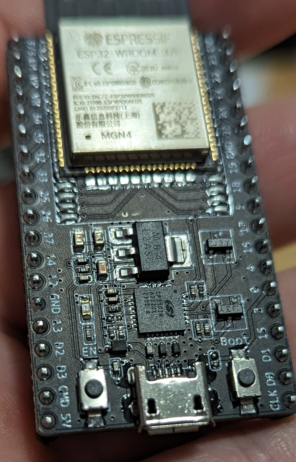
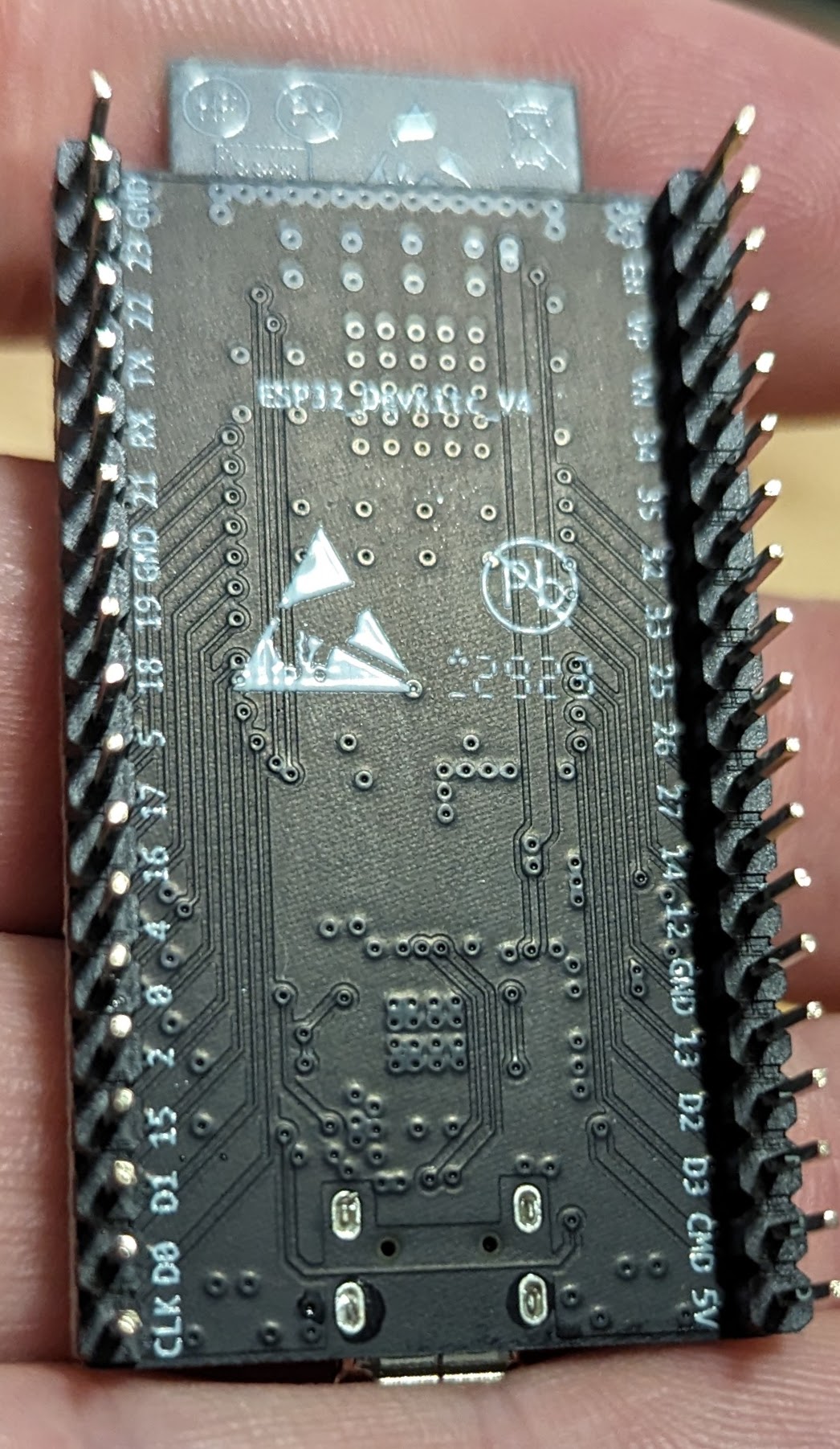
This is a dev board, so something that might be good to put in, is to break out the GPIO on the CP2102-N.
Why, you might ask? Well- it is a dev board and you might sell these independently.
But, even for your own use, you may be able to use the GPIO for your own tests. For example, use them for self-test of the jackpot. (stimulate the endstop switches, or the GPIOs, or even make test adapters for the polulu sockets…)
You don’t necessarily need to fit header pins them in all boards built, just leave solder pads or through holes so that they can be populated if/when desired.

Be careful about this- cheap USB/Serial bridges are a source of much pain and suffering! I’m pretty happy with the 2102 being on the boards supplied with my Jackpot.
1 Like
How do you use these, if they were broken out? As in, are they just USB accessible?
This chip also has a built-in voltage regulator, that we don’t use.
The bummer is there is very little room for breaking things out like this, that chip in particular. There is some room though.
Not necessarily cheaper, just fewer pins not used. There do seem to be a couple popular types out there.
Not tying to make any significant changes to the design until I really understand it better. Most of it I don’t fully understand.
Yes, from the USB host side you get access to that GPIO. You can do all the usual GPIO stuff from the host.
So, aside from programming the device, you could for example use the GPIOs to drive high or low on demand, and there are 2 UART interfaces there. Lots of debugging stuff you could do from the host side.
1 Like
You’d normally have some form of PC program that controls them. It’s pretty simple to do, under Linux you can do it straight from the command line even. Silicon Labs have an example program that I’ve started from before but if you were trying to do something super basic you could almost use it as-is.
In this case it’s just very basic high level programming.
That’s a good idea, I quite like that.
1 Like
That looks pretty reasonable. Nice and clean.
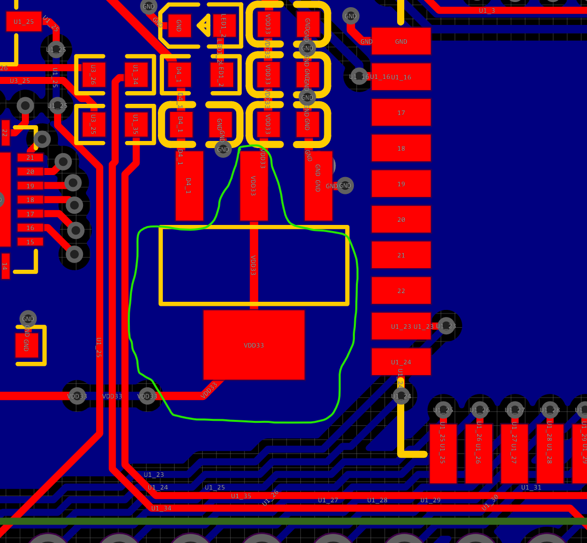
Looks like the linear regulator is a different part. SG Micro SGM2212-3.3:
Still has that annoying layout with the tab connected to Vout. Hideous.
That one is not available on LCSC, when it was, it was $1 vs $0.03. There are a bunch I can’t find any that have the tab as ground though.
I think I got most the suggestions, I have not done the ground stitching yet, that needs to be last.
The two 0 Ohm resistors on the TX and Rx lines, I tried googling that. I don’t really understand it. Are they really needed, one of the reasons google cited is to act as placeholders.
Oh, and you are sure C5 is not needed?
After seeing this built, I really want to move the jackpot coms pin off gpio0, that pin has soo much going on.
I was able to squeeze them in, I need to place some solder pads on the bottom.
3 Likes
Yeah, that’s the general idea, although the space under the device isn’t really going to do as much as the space on the top surface. It will still help a bit because some heat will get transferred to the ground plane through the fibreglass itself, but the main goal is the area around the tab. I’d fill in that entire zone there with copper, all the way out to those other traces.
It’s really just acting as a heat-sink. The more area you can give it the better, up to a point, because it means the regulator will run cooler and have more headroom to cope with short term overloads. To determine how much you actually need, you’d need to work out the power dissipation from the current draw and supply voltage.
Usually it’s a case of either provide overkill and don’t bother calculating it, or if it’s likely to be marginal then make sure it’s calculated reasonably accurately.
If all the 3.3V loads are taking ~200mA total then running off 5V you’ve only got 340mW (5V - 3.3V so 1.7V drop across the device, 200mA at 1.7V is 340mW). Unfortunately the datasheet doesn’t give a reliable thermal impedance for the bare device, which is pretty slack. It just say >90degC/W. It gives a resistance of 80degC/W with 100mmsq on top (10mm x 10mm) and 2500mmsq on the bottom (50mm x 50mm), so that looks like it’d be well above that. Assuming 120degC/W that puts the temperature rise on that device at 41 degrees C, roughly. That’s easily fine and assuming a 50 degree C ambient (bearing in mind that ‘ambient’ in this case is likely inside an enclosure shared with some toasty stepper drivers and with potentially poor airflow) because that will mean the chip itself is running at 90 degrees C when it can run up to 150.
If you try running off 12V then that 200mA is now 1.74W and that same thermal resistance gives a 210 degree temperature rise, so there’s just no way. Working backwards, assuming you want 20 degrees of headroom from the chip being at maximum temperature, that’s 130 degreesC working temp. With a 50 degree ambient that’s 80 degrees of headroom. At 120 degrees C per watt, that’s 670mW maximum dissipation. Running off 12V that’s 78mA. As long as you’re drawing less than 78 mA you’ll be fine.
I don’t actually know what one of these draws. That might be worth measuring? Unfortunately with microcontroller type applications you’ve really gotta measure it while it’s doing stuff, though.
About 80% sure. Looking at the diagram there are 2x 100nF capacitors in parallel and they’re just providing debouncing/filtering for the enable line, which is an extremely non-critical scenario. I think they’re just added an extra 100nF cap across the switch without thinking about the fact that there’s already one on the line elsewhere. If it ends up being a problem, you can always replace that 100nF capacitor with a 220nF capacitor with minimal effort.
Yeah, my personal approach has always been to avoid any of the bootstrap pins, where possible. I think we had that conversation a while back when doing the Jackpot. They’re just extra complication and mean you’ve gotta be careful about what’s on them from the perspective of startup and where the lines get pulled to, logic-wise.
1 Like
So would mirroring it on the bottom and VIA stitching help? On the ones I have here, the ESP module is by far the hottest component. I will check again but the VDO barely gets warm from what I remember.
I will look again, the close /easy one is a module pin. 90% unused, but when it is it could be an issue so that one is a no. I will look at what is next to it. I will follow up in the other thread but the esps I thought were “bad” work fine with the steppers plugged in so the pull-up we added was not a 100% fix just a lot better than before.
It would, but not necessarily ‘that’ much. It creates a big discontinuity in the ground plane in that area so you’ve gotta be careful to consider where the return current for other traces will run. The top copper will also already transfer heat to the bottom plane through the fibreglass. It’s technically an insulator, but you’re talking about a relatively thin insulator with a lot of surface area connecting them and not much actual power. Also the bottom of the board is likely to be worse for power dissipation in most orientations. If they’re not getting warm currently then I wouldn’t worry about it too much. In the ESP32s I have around the house, the ones running off 12V were hot enough that it was concerning from a longevity/functionality standpoint. That’s one of the reasons I made my little break-out boards with a DC/DC converter to power them from 5V.
1 Like
Yeah, I was looking yesterday. I can’t tell if a bunch of parts have gone obsolete and disappeared or what, but we’ve used a ton of different voltage regulators and always had ones with grounded tabs. Now it was just a rare few. The cost thing is always going to be a problem you’re going to run into. This is one of the huge things that can drive a wedge into the cost of products. There are cheap devices made by companies where they’re not necessarily doing the same level of QC/development/documentation or there are expensive devices where they focus strongly on their reputation and put a lot of effort in. One of the skills is being able to take a step back and evaluate how important each component is from a design standpoint and pick accordingly. All my sideline products are intended for high reliability environments and cost isn’t as sensitive so I tend to only use components from western manufacturers for anything active/silicon based. The passives from Chinese companies tend to be good enough for my purposes so I use those. If I were designing for a different scenario, I’d likely use Chinese diodes, LEDs, whatever but leave the core functional pieces western. If I were aiming for rock-bottom price, the only realistic option is all Chinese components, accompanied with the acceptance that there’s likely a larger band of uncertainty around the performance and that some extra design validation might be needed.
It’s also important to note that Chinese components here really mean components wholly designed and manufactured by a Chinese company, because the vast majority of western companies are still manufacturing in China to some significant degree, anyway. It’s more of a questionably accurate generalisation about the goals and motivations behind how those companies fit into the marketplace than it is about anything specific to a location of manufacture etc.
As an example, just a week ago we had a team from Infineon come in and present a bunch of their research into design and lifetime prediction for high power switching modules. Even within well-known western manufacturers there’s a huge spread in how much R&D that gets done and how that gets communicated to the customer. In Infineon’s case, I’m not a huge fan of their devices because they tend to have slightly worse performance at a higher price point, but that’s offset by the knowledge that they’re definitely telling you the whole story and have done the research to uncover specific failure modes in the past that affect all forms of that technology, not just theirs.
Yeah, there’s seldom a reason to put a 0R resistor somewhere other than as a placeholder, so they can be safely omitted if they’ll never be changed. The reason you’d put resistors like that in series are so that you’ve got the ability to add impedance in case there could potentially be multiple driving sources on that one line, or in case you need to slow down the edge rates of a digital line for EMC/EMI reasons.
From the multiple driving sources perspective, it likely depends on the behaviour of the CP2102 and how the design is being used. If you wanted to use the TXD0 and RXD0 on the ESP32, you’ve potentially got a situation where 2 chips will be trying to drive the ESP32’s RX pin. Having a 100R resistor there means that even in that case, one chip will likely ‘win’ and just ‘shout over’ the other, without causing an issues. With a 0R there or no resistor, chances are you’ll get excessive current draw, no usable signal, erratic behaviour and potentially even damage something. I haven’t looked into it too much, but my suspicion is that the CP2102 might put it’s TX/RX pins into high impedance mode if Vbus isn’t present, so the only way that would occur would be if you’re using TX/RX on the Jackpot and also have the USB plugged in. That’s speculation for now, though.
From an EMC perspective it’s typically best practice to have some form of impedance between digital inputs/outputs. All inputs have some amount of capacitance, as do all circuit traces. A fast-changing digital signal causes a big pulse of current into those traces that then radiates as EMI. Having a 10 or 100 ohm resistor there significantly limits the magnitude of that current pulse. Having a 10R resistor and something like a 100pF or 1nF capacitor is even better, as you’ve then got a deliberate RC filter to slow the edge rates down, but that’s starting to become a lot of components. Often you’ll see what is basically an RC filter attached to a digital output but with the resistor being a 0R link and there being no capacitor fitted. That’s because it’s easy and cheap to add the positions for the components at design time and then change the fitment later if it turns out they’re needed, rather than needing to re-spin the entire board.
That seems to be worth a lot.
So leave them, change them, or delete them. I can look to see if the cp2102 has something built in.
They do not cost anything but another component to the feeder charge. If they have gone all these years without them, it would be safe to say a placeholder is no longer needed.
As with anything it depends. If you’re trying to wring every last bit of performance or longevity out of a device, it’s hugely important. If you’re trying to do something a little more basic, it’s meaningless.
The specific example there was talking about failures in power semiconductors due to thermal cycling. This is especially important for vehicle charging applications because it’s an intermittent load. You’ll go from sitting at ambient, unused, to running at full power for ~15-30 minutes and then drop back to ambient. That might be power semiconductors going from 30 degrees all the way up to 150 degrees and back down several times a day. On top of that, there are small thermal cycles every time the device switches on and off due to the thermal impedance of the packaging. So it’s a daily cycle of maybe 10x big swings of ~100 degrees and then billions of small swings of maybe 3-4 degrees.
They’ve characterised all of that so that they can attempt to predict lifespan before the bond between the chip and the substrate fails. This is helpful because without this information, the natural tendency is to let the device run as hot as possible, because that’s when you’re getting the most performance out of it for your money. Running it at 150 C internally means you can get away with a one specific device while running it at 100C means you need either a much more efficient device or more devices in parallel. It may be the difference between having $200 of power semiconductors in a design or $400. If you can find out at design time that the $200 option will likely be dead within 5 years of worst case conditions given how you’re using it, that means you can then decide how to approach it. Either just beefing up the devices used to extend the lifespan, lowering the specs on the device to keep it alive longer without changing it, monitoring the operating conditions and providing a ‘lifespan estimate’ so you can forward-replace the units that are getting hammered. That kinda thing.
That would be my approach. I can’t imagine a world where you’re suddenly going to decide that you need to change them and even if you do, you’re unlikely to be doing that personally.
1 Like
Thank you for all the help.
P.S. I am addicted to this stuff. It is more fun than Tetris. I messed with it for another several hours last night. I want to do it all over again, I think I can make it nicer with a shifted layout.
(I even started a TMC2226 driver)…
1 Like
That’s awesome! I’m not sure if your experience will follow mine, but I’ve always had a ton of boards that I’ve designed and then never bothered to get made etc. or ended up throwing out and restarting for a bunch of reasons. Sometimes it’s a case of doing all the work and then ending up with it not being practical or having problems that are annoying to solve or compromise the design. Sometimes those just need to be stewed on for a while to come up with a solution, or to make peace with the compromises involved. Whatever the case, it’s all learning and improving skills which make the next one easier.
As with anything, there’s no one true route through all of this.
1 Like