I’m very interested in a PCB kit as well. I’m sure many others here also have most of the components needed besides the custom boards and aluminum plates.
1 Like
Okk just published the PCB kit:
Came out to a little more than I was expecting. Forgot to include tariffs on that initial estimate ![]()
Ordering in the next day or two, so the lead-time should be around 1-2 weeks.
2 Likes
Thanks for the update! Just to clarify—when you say not all of the components populate in the correct orientation, are there specific parts I should double-check more carefully?
Also, since this is my first time doing this: what’s the best way to verify that all components are placed in the correct orientation and position? Is there a visual reference or template I can use to double-check the layout before assembly?
The small IC, polarised caps and stepper connectors needed adjusting for me
2 Likes
Thanks, Picklez, for the helpful reply!
Would it be possible for you (or anyone else) to share a photo of the JLCPCB order showing the component placements?
I’m especially interested in the positioning of the small IC, the polarized capacitors, and the stepper connectors. That would help a lot!
Thanks in advance ![]()

Here’s a photo of my current setup for reference.
It might help show what adjustments I had to make or what’s still unclear.
Any feedback is welcome!

Just for me – and maybe for others as well – and to wrap this topic up:
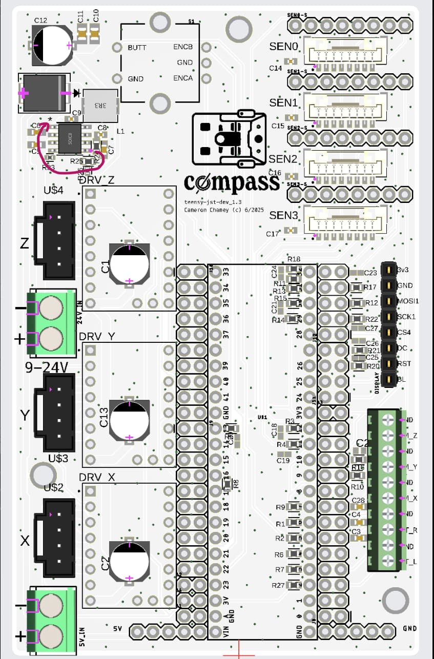
Regarding the PMW3360 PCB , apart from rotating the SOT-23-5 by 180 degrees, is there anything else to watch out for with the other components?
Huge thanks to Picklez for your support, and greetings from Hamburg!
I haven’t looked at this pcb in detail, but just look at this with my electronics manufacturing experience:
The footprints for the capacitors and resistors look too big to me for the parts used. The footprints look for example like footprints optimized for hand soldering.
When you use this kind of footprint for reflow soldering instead, there is a steep increase of probabilty that tombstoning happens. The solder paste melts at a slightly different point in time on the two sides. The surface tension gets larger depending on pad size. The side that melts first now exerts it’s surface tension on the part and that can lift up the part from the other side that is not yet melted.
So I suggest to either increase the part sizes or decrease the footprint sizes. The latter is probably cheaper when you target PCBA-services like JLC, because the smaller parts are often more common.
Just to be clear, I meant the screenshot of the PMW3360 PCB as shown by JanOetjen.
Hi there!
First of all, thank you for making this project open source—it looks fantastic! I’ve ordered all the hardware components and, as a mechatronics engineer, I have a few suggestions to improve the PCB design. I would be happy to assist if you share the project files.
-
The pads for the SMD components appear to be oversized, even larger than those for hand soldering. This could lead to assembly issues.
-
While the specified model of the step-down regulator is functional, I would recommend considering alternatives for this application. The current model requires some unusual resistors and capacitors, which can increase the cost of the assembled board—especially since JLCPCB charges extra for parts from their extended library. A better option might be the TS2596CM550, which is affordable, readily available, and only requires standard components. Though the TPS54360 supports input voltages up to 60V, 40V should suffice for most applications.
-
I suggest using Molex JST XH insted of the pin headers. There are many very cheap copies available in the JLCPCB library, and they are considered an industry standard. They allow for easy sourcing of cables and would be a more effective solution than pin headers for this purpose.
-
For power connections, I recommend using Phoenix Contact MC 3.81/3.5 series connectors. These are also widely available in the JLCPCB library at a low cost (copies) and are common in the industry.
-
Are you using UART or SPI for the Teensy 4.1 and TMC2009 communication? Implementing sensorless homing can reduce the need for additional cables, and using UART provides numerous advantages, such as the ability to adjust the stepper motor’s amperage through software.
Best regards!
1 Like
Hmm yeah it’s weird they do seem big. This is just the standard 0402 footprint for the capacitor library I used. Must be made for hand soldering. I just switched the library for all the parts on the sensor board and the footprints are much smaller. I’ll be using this for manufacturing and will upload the files to the repo soon.
Awesome, thanks for all the suggestions and excitement for the project!
That sounds pretty solid. Being able to accept 48V could be a good options to have for future upgrades, but I will definitely consider it.
Are you referring to the display header? Yeah, I’m definitely planning on switching this at some points. But for now it’s easier to be able to use dupont connectors so that you can use a variety of different off-the-shelf displays with different pinouts.
UART yeah. Sensorless homing is definitely on the to-do list! Just have a few higher priority things to get to first ![]()
oooh i’ll have a limited edition chonky pad one, my PCBs are in the post ![]()
2 Likes
Hahah lucky duck. They will be fine. I’ve been using chonky pads for the past ~100 sensor boards I made
@camchaney I’m seriously in awe of this project — it’s incredible work! I’ve just started building one myself and got a PCB order underway through PCBWay. It was a bit tricky to set up at first, but I’ve now finalised the boards. Like others have mentioned, ordering 10 boards isn’t much more expensive than ordering one — so I went for the batch.
Would you be okay with me offering a few of the extras to other Aussie makers at cost price, if anyone needs one?
I’ve attached the final BOM from PCBWay if that helps others too. These boards come with assembly from PCBWay however I chose to install the PMW3360 myself and not quoted in these PCBWay BOM. PCBWay don’t seem to have a reference for part numbers they stock so can be tricky to organise.
PCBWay BOM.zip (45.3 KB)
Also, just checking — are there any planned changes to the board design I should be aware of?
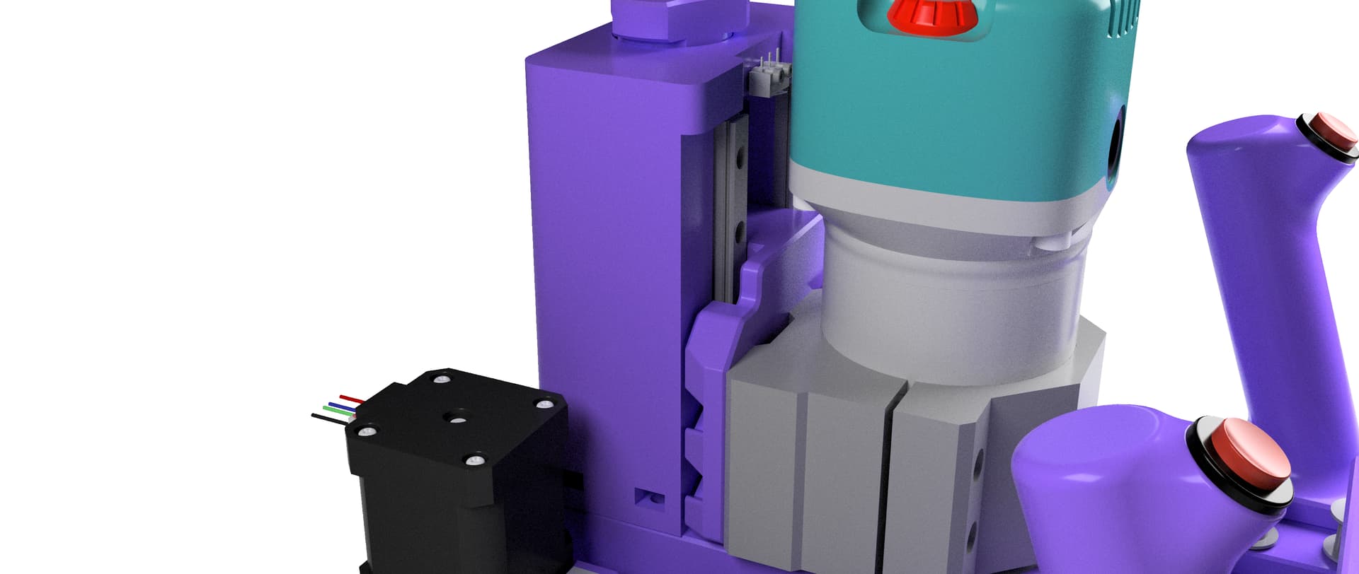
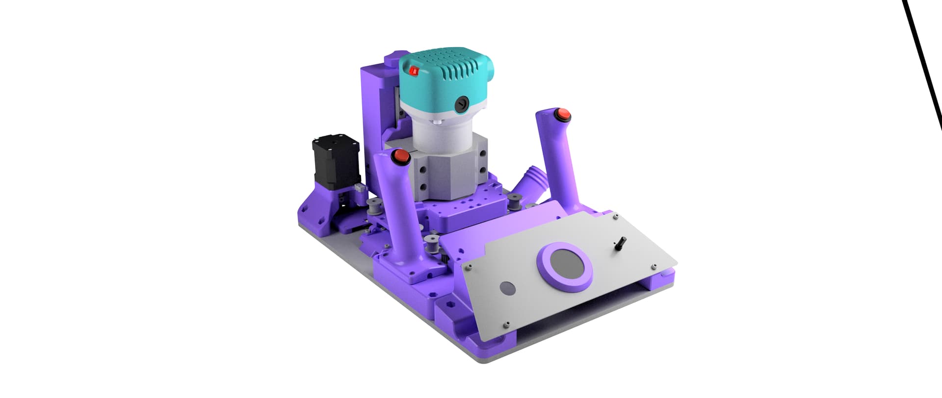
Lastly, I’m planning to tweak the Z-axis design slightly to use linear rails and an aluminum spindle clamp. I’ve had some issues in the past with plastic parts deforming due to spindle heat. Is there a preferred place you’d like me to share those updates or mods?
Thanks again for all your amazing work on this!
Yeah for sure, go for it.
Nothing for the near future.
Sounds cool! That’s a great question. I would say for CAD remixes (mainly 3DP stuff), post them on your printables (or your preferred 3D model sharing site). If there is enough interest for that specific remix, I will add it to the repo
Thank you for your response @camchaney
I have had a play with the z axis linear rails and a common beefy aluminum spindle mount. Let me know if you see any huge issues?
I have uploaded my files to my thangs if you want a closer look!
https://thangs.com/designer/newtechcreative
Did you consider using the PAW3395DM sensor? Seems like it has higher accuracy and cost wise not much difference. However, I’m not an expert in these sensors, so I’m not certain if´I’m missing something and that would actually improve accuracy.
I would greatly appreciate it if you could share the PCB files. I would be happy to adapt the design and potentially create a version for the PAW3395DM. I have received all the components and printed the parts, but I haven’t ordered a PCB yet because I would like to modify it to better suit my needs. Providing the files would save me considerable time and effort in reverse engineering the design. Thank you in advance for your help!
Oh sweet! This isn’t essential, but moving the linear rails further out to the side to make the router less cantilevered would make the system a lot more rigid. That would be easier with a 3D printed router mount instead of the beefy aluminum. The beefy aluminum part won’t offer any rigity advantage if the part that’s holding it isn’t rigid itself.
Also it looks like there isn’t actually a hole for the lead screw to go through.
Cool concept so far though!