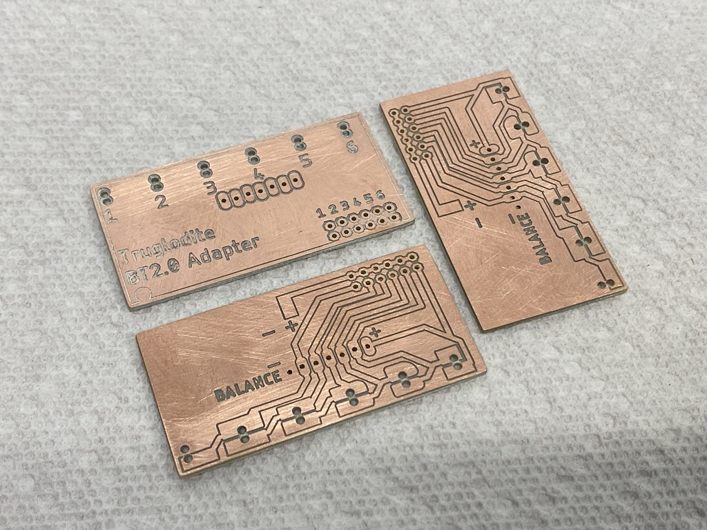
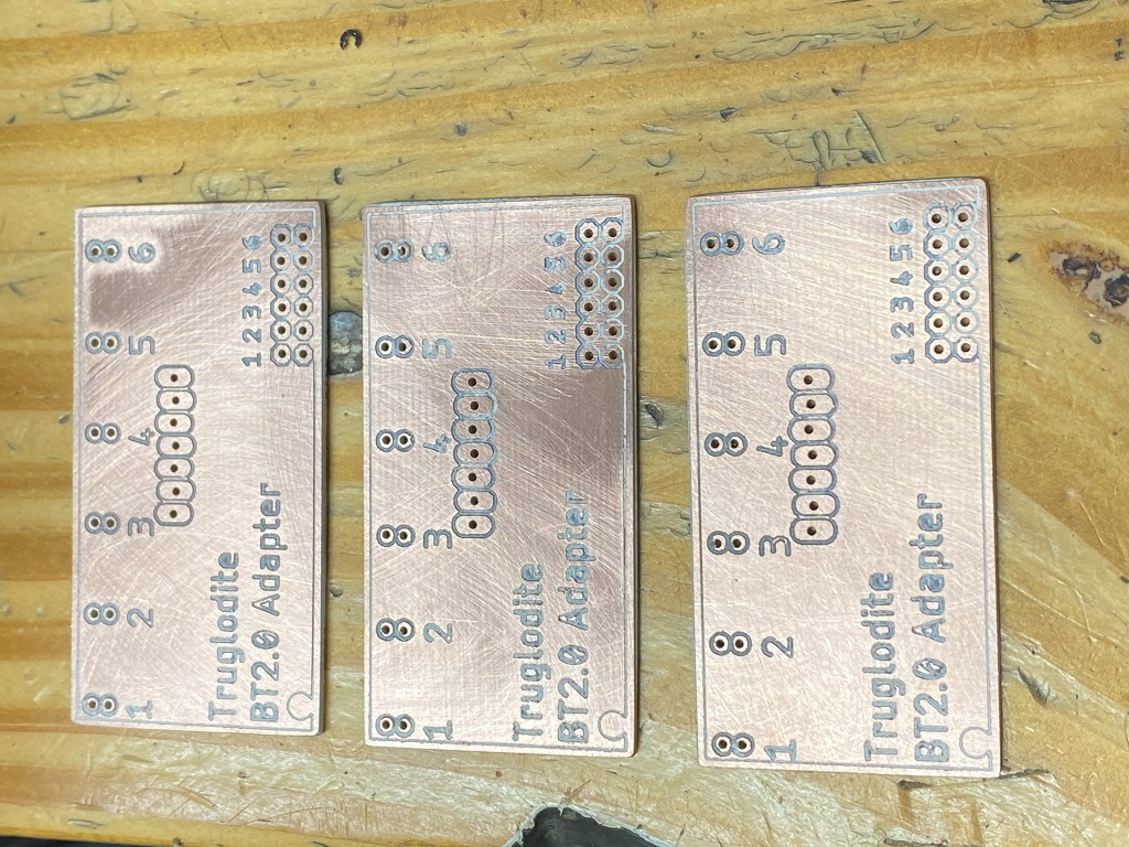
Here is another PCB I designed with Eagle+Fusion360, and milled/drilled on my MCPCNC primo. They turned out decent despite having some struggles with customizing the footprint for the BT2.0 connectors. I ended up using polygons and net classes to get that done, since I couldn’t for the life of me figure out how to make a pad with an offset hole in eagle.
The boards are milled on both sides. I used drilled holes as registration marks to line up the flip side with a drill bit. I made a custom pcb flip gcode script (spreadsheet actually), to generate the gcode I use to move between registration marks. I can elaborate on this process if anyone is curious. I also made use of bCNC surface probing, to correct the gcode for the wavy surface. Surface leveling is IMHO the most important ingredient in making decent milled pcb’s.
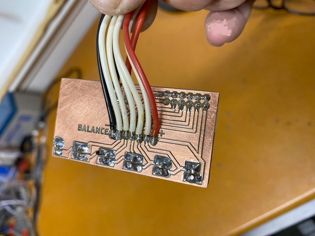
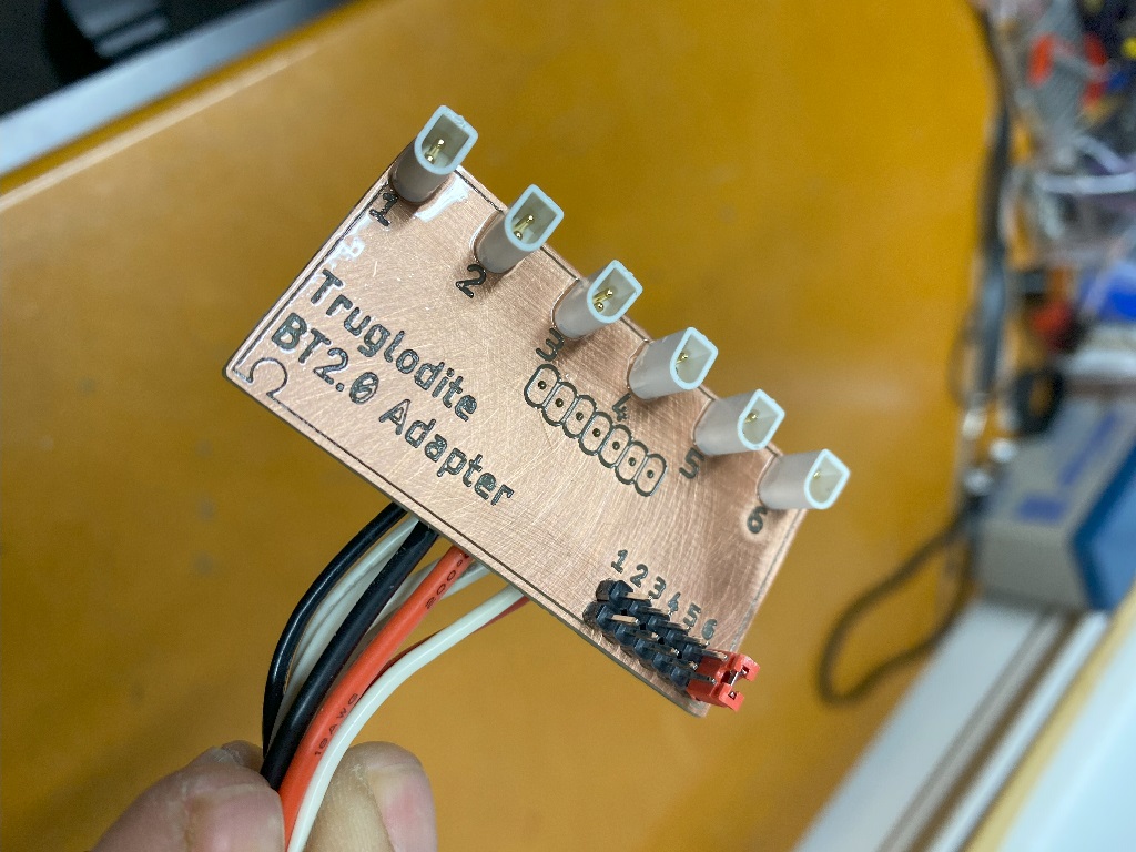
A variety of similar charge adapters are commonly found affordably priced at the usual online retailers, but since the BT2.0 connectors are so new, I haven’t found any similar devices with them (just JST-PH or GNB27). BT2.0 connectors have become all the rage among folks who fly Tinywhoop drones, and my entire fleet of 1s aircraft uses them. I did already have a Whoopstor charger that is a far more valuable tool, but I wanted to be able to also use my 2 big lipo balance chargers for certain situations… like when I fly a lot, or when I change my mind about flying 65mm vs 75mm. I used a set of jumpers to select cell count instead of a rotary switch. This saves cost, kept it simple, and made it way more reliable.
Riley I’m not sure if estlcam can do it or not currently. When I initially was setting up to cut PCB’s a couple years ago, bCNC was AFAIK the only option available that didn’t require a lot of work to implement leveling. What Jeff said is pretty much how bCNC does it. In a nutshell… load up the original gcode, go to the gui tab for probing/leveling, hit some buttons on the gui, it probes the surface, hit another button to “modify” the loaded gcode using the leveling data, and cut away. TBH even if there were other solutions at this point, I’m satisfied enough with my f360+bCNC workflow that it would take a lot to make me change (like 4th axis a lot).
Thanks Ryan… this time I was actually impressed with how thin and perfect that border etch line came out. The other traces/marks are mostly doubled up cuts for easier soldering. After the cut though, I saw the details inside the letters, and that thin rectangle… got me thinking this rig might actually be able to do some decent SMD boards (at least QFP, not sure about QFN though).