The box of traces they have makes ?e wonder about the durability of the circuit but it’s a great video. I have thought about conductive printing ink first but not as dramatic ![]()
Yeah, that box of traces was hilarious. At least it’s basically just pure tin. Easily melted into a solder pot for tinning usage etc. We’ve got a couple kg of it at work in tablet form for the solder pots.
I was wondering about the conductivity of the solder. Tin is 15% IACS but then a standard PCB trace is only 35um thick and usually ~0.2-0.5mm wide, so I suspect they’re probably in a similar ballpark at what looks like 1mm wide and 0.3mm tall.
I’ve never worked with conductive ink, that’s an interesting idea. MG Chemicals has some for EMI/RF shielding which I should really grab a tub of, that sounds useful. 530uR.cm compared to 1.7uR.cm for copper is a yikes. It’s specified in a 50um thick coating so a 300mm long, 2mm wide trace of it would be 16 ohms… Hmmmm. Potentially ok if you’re putting 10mA into an LED, I guess.
1 Like
Food for thought and small traces ![]()
1 Like
Some people actually care about where their data is stored. ![]()
2 Likes
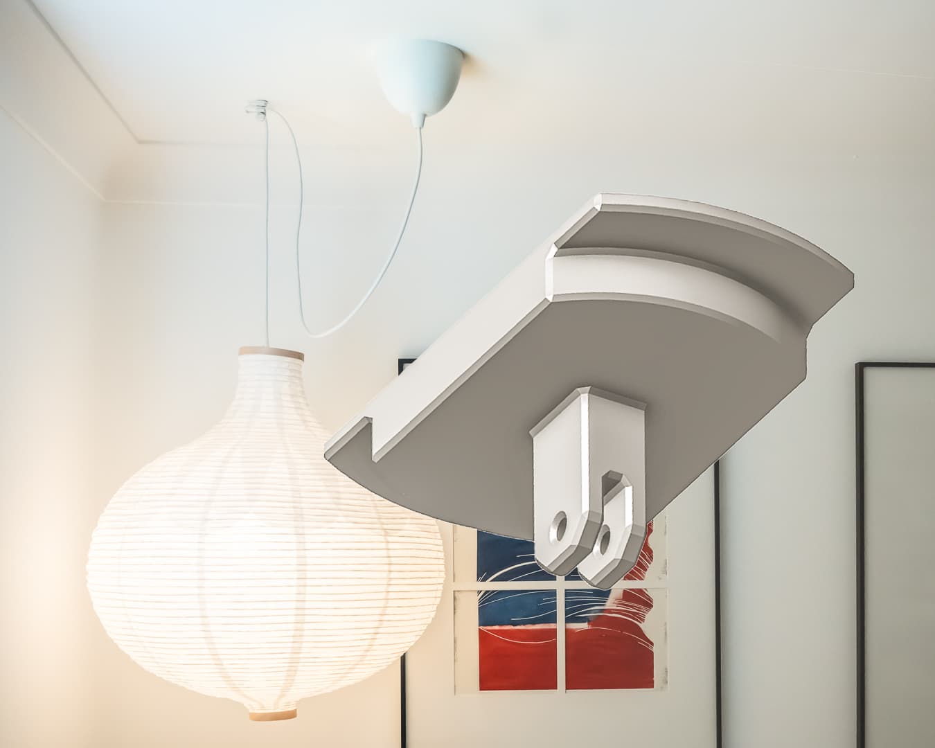
I was going to start a thread called " things I’ve been doing that are keeping me from starting an LR4" and I still might, but this worked out well enough to be “neat” I think.
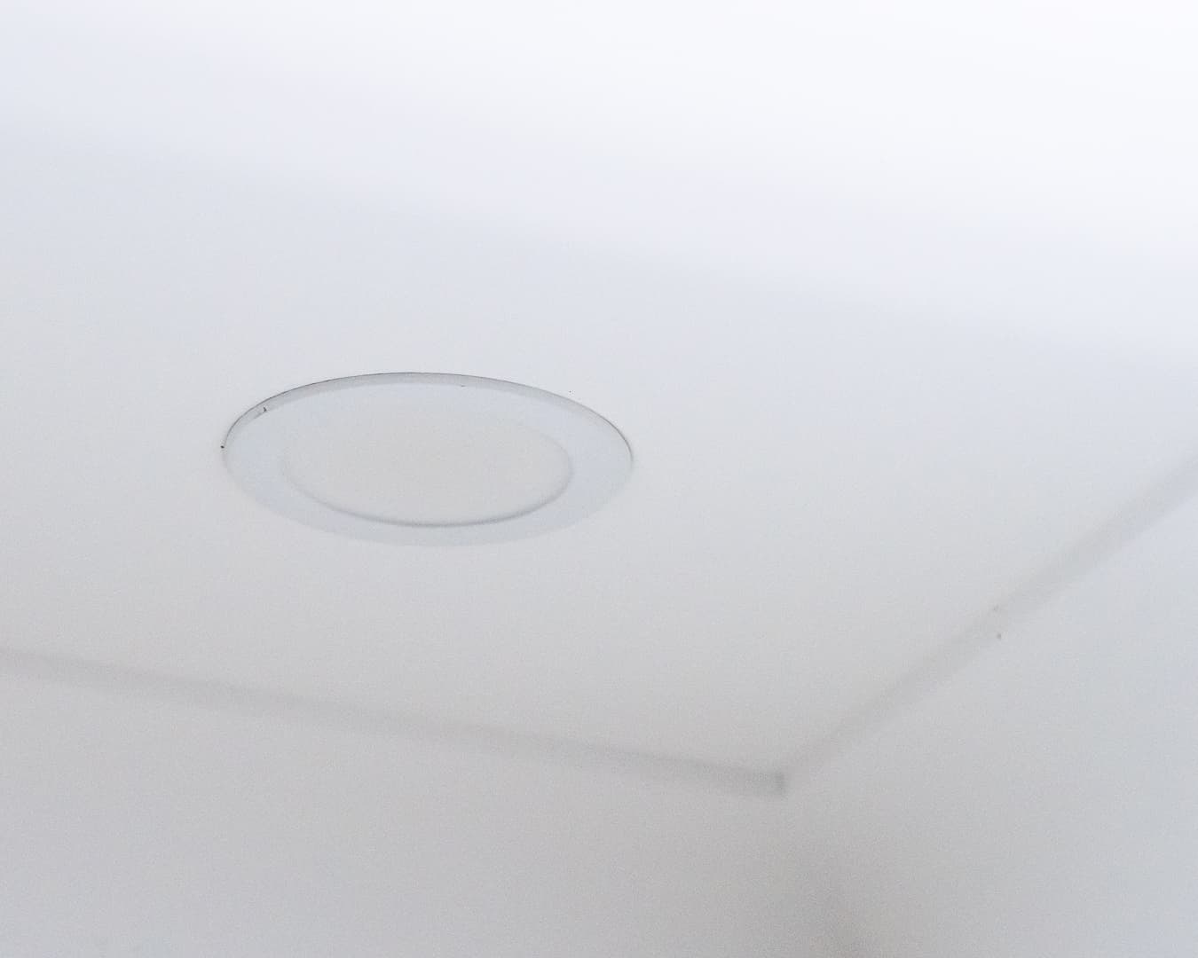
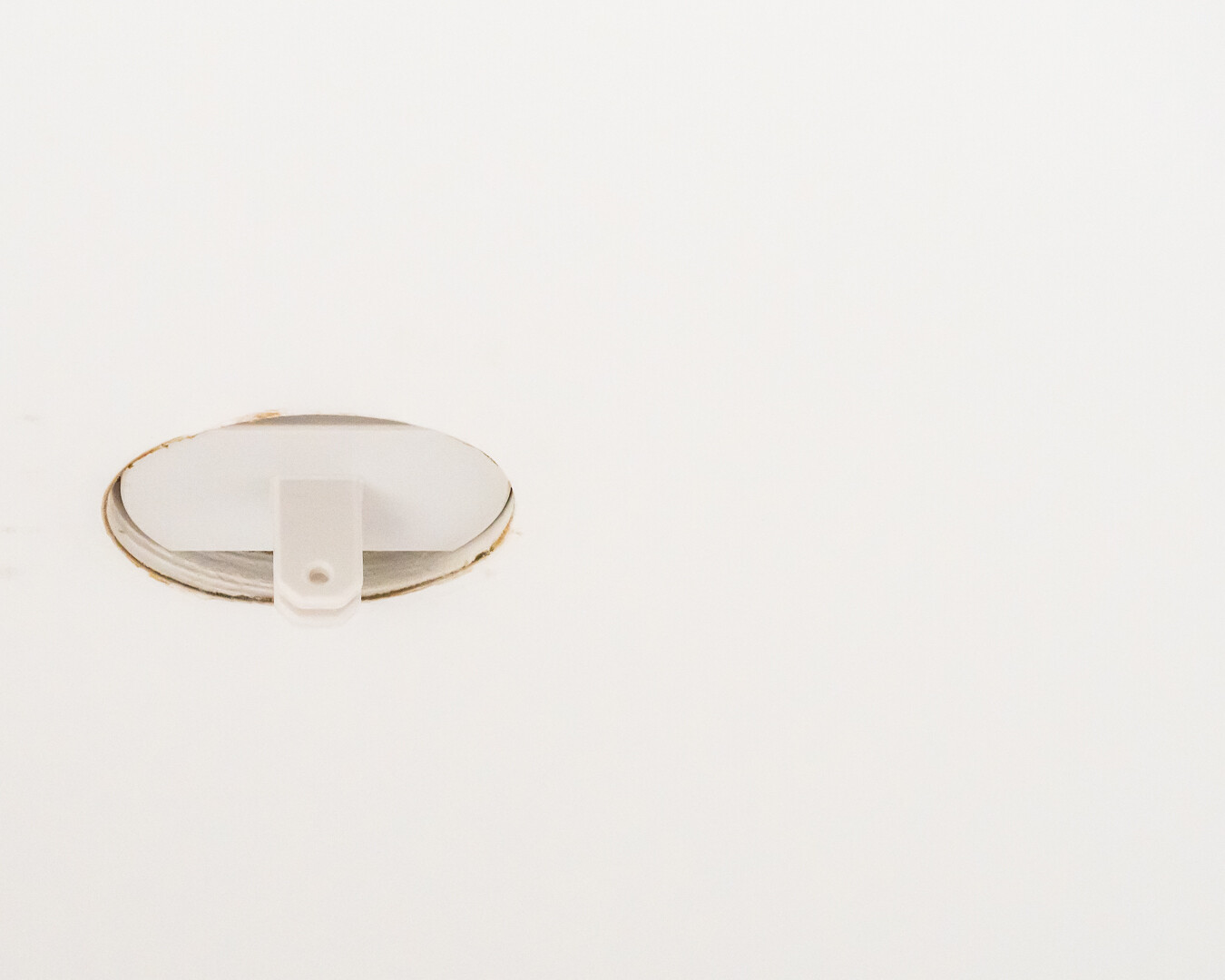
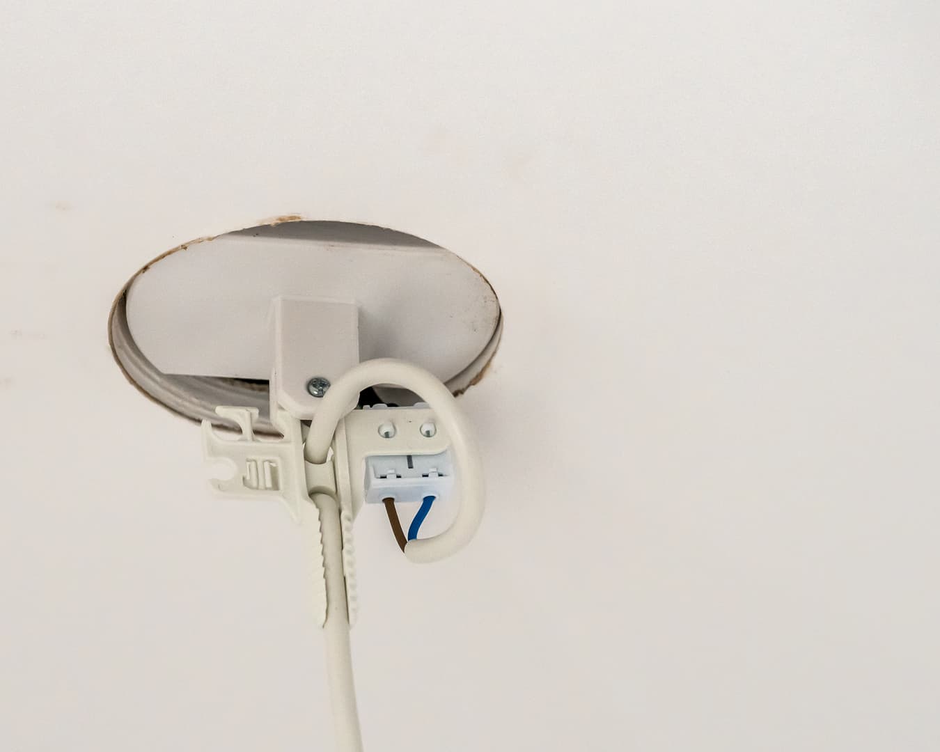
We had a blown LED downlight, so why spend $10 replacing it when you can spend $50 and stick a pendant light there.
I printed a hook that neatly sits in the downlight hole so there was no need to repair it, and we can always put a downlight back there if we need it. It’s just one of those simple solutions that make everyone happy at the end of the day!
Yes, it’s on Printables
if you happen to have a broken downlight and an IKEA light fitting in your cupboard, you can play along!

7 Likes
Could always chuck it up in the ‘things I’ve made’ section. That’s a neat idea.
2 Likes
I always think that’s for things made on the CNC??
1 Like
I’ve always assumed it was more generic than that. At least there are some V1 3D printers around, too. I posted my gamepad project there, although that did get a CNC’d wooden housing eventually.
1 Like
Did i miss that? Sounds cool

Main goal was to make something ortholinear to hopefully prevent some finger strain. Ultimately I didn’t end up using it for more than a few weeks because even after getting used to it the aligned number row kept tripping me up with weapon switches while moving.
2 Likes
How is this the first time I’ve ever seen someone using solder as filament. Thinking about it, shouldn’t anyone have thought about this way sooner? I’m guessing as long as you get the right diameter solder, you could do this with any direct drive 3D printer.
1 Like
And if you don’t, you could have built-in fuses! It reminds me awfully of fold fashioned wired fuses I’m afraid.
incandescent light bulbs? ![]()
1 Like
I think my next keeb project is going to be this one:

I prefer 5 rows. So I may have to design my own.
2 Likes
Looks pretty neat. That’s a tidy setup.
I still think I’d want to do a PCB based one. The hand wired ones, even the neatest ones just look like an absolute nightmare.
So could the printing of solder be used as a way to run electrical traces through a print job? Just have the solder as another spool of ‘filament’ and then it is another ‘color’ that the printer swaps in and out. Have your 3D prints with imbedded wiring would be a whole other level I would think, no? You could then imbed lights and other items right into the prints. Not just hardware.
Philip
1 Like
@jono035 is far better qualified than I am to comment on this, but while that’s a very cool idea, I think it would add a whole other level of unreliability and even uncertainty to the circuit!
2 Likes
That’s definitely an interesting idea that hadn’t immediately occurred to me. That could go a long way to dealing with the ‘why’ approach.
There are conductive 3D printing filaments that allow some things like this and companies that provide this functionality using things like SLS prints etc.
The conductive filaments aren’t really what I’d call truly conductive, they’re more along the lines of ‘not insulative’. Looking at the specs it looks like 1-10 ohm.cm (compared to tin at 10 uOhm.cm) is about as good as it gets according to the spec sheets but the reality of a printed parts seems to be noticeably lower, potentially up to 10x or worse. In that range of conductivity you’re talking very low power circuits, static dissipation or touch sensing types of duties rather. Things like strain gauges, perhaps, but probably not enough to reliable run LEDs beyond maybe a high efficiency element as an indicator. A 10cm long trace running an LED at 10mA would need to be ~1cm², for instance. It’s similar to the ways that conductive ink is used.
We’ve investigated using the SLS approach before at work for embedding sensing coils into the surfaces of mechanical protection/weatherproofing housings, although we never went through with that part of the project. They were printing copper powder directly so were getting a relatively high fraction of the conductivity of copper but even then it was a bit of a struggle to get conductors with high enough Q (low resistance vs inductance) for our needs, compared to a conventional PCB but probably fine for a ton of other tasks. It was also hideously expensive, but that may have been a side effect of the size that we were looking for, too.
My gut feeling with using solder directly in a multi-material print is that it would be possible but likely have a bunch of complications that may make it difficult.
My first thought was that the tin likely has much higher thermal mass which could cause it to melt into the material around it rather than staying in place. Oddly, the thermal mass of tin seems to be roughly similar to most filaments, volumetrically speaking, which still doesn’t seem right to me. Specific heat capacity of 0.22 J/(g.°C) and density of 7.3 g/cm³ so 1.6 J/(cm³.°C) vs PETG at 1.2 J/(g.°C) and 1.25 g/cm³ so 1.5 J/(cm³.°C). So I guess that’s not likely to be an issue.
Another wrinkle was that they were printing with fluxless solder which will create a pretty nasty oxide layer pretty much immediately. That’s not so much of an issue if you’re going to print it as a continuous trace and then connect to it using a fluxed solder but may be an issue with getting layer changes to reliably join together. That could be solved by potentially printing slower to allow more energy to conduct from the nozzle to the previously printed filament but there’s still potentially an oxide skin that may not be disrupted enough to create a reliable connection. That’s potentially solvable by using a purge gas or something, though, or a formulation of solder that forms weaker oxides or forms them more slowly.
I’d guess that purging the old material through the nozzle might not go well so it may suit an IDEX or toolchanger machine better as an approach.
So yeah, definitely an interesting possibility.
1 Like