as long as we don’t have to blow on it to connect
That was the best part, “just for luck”, if it worked the first time, it was going to be a good session.
2 Likes
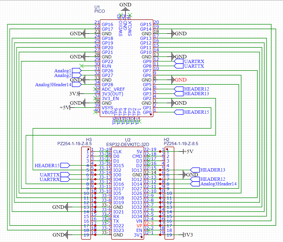
Pi Pico to ESP32 - EasyEDA open source hardware lab Here it is so far, if any of you want to double check my work.
I still need to add some flair and pin labels.
They are looking like they will be $10-$12 I was just going to grab 5. If any of you are interested in one let me know. If any of you are interested in making the TMC expansion work in klipper I am extra interested…let know.
For labeling the pins, what would be best to put there, where it goes on the jackpot, the pico pin label, the esp32 pin equivalent?
2 Likes
some orientation que would be most helpful to make sure it is plugged in correctly… maybe have text read the same direction as the jackpot when installed correctly? as far as pin labeling, any of the breakout pins or connectors should be labeled. I would like silk screen on the bottom with the pico pin labels so if it isn’t plugged into the jackpot it can be used to prototype without having to consult the schematic, though that is readily available online.
I’ll see if I can rough in a printer.cfg file for the klipper setup. If this is for the V5, most of it is on the v4 nearby, I just need the pin names for the pico and we are pretty much there.
1 Like
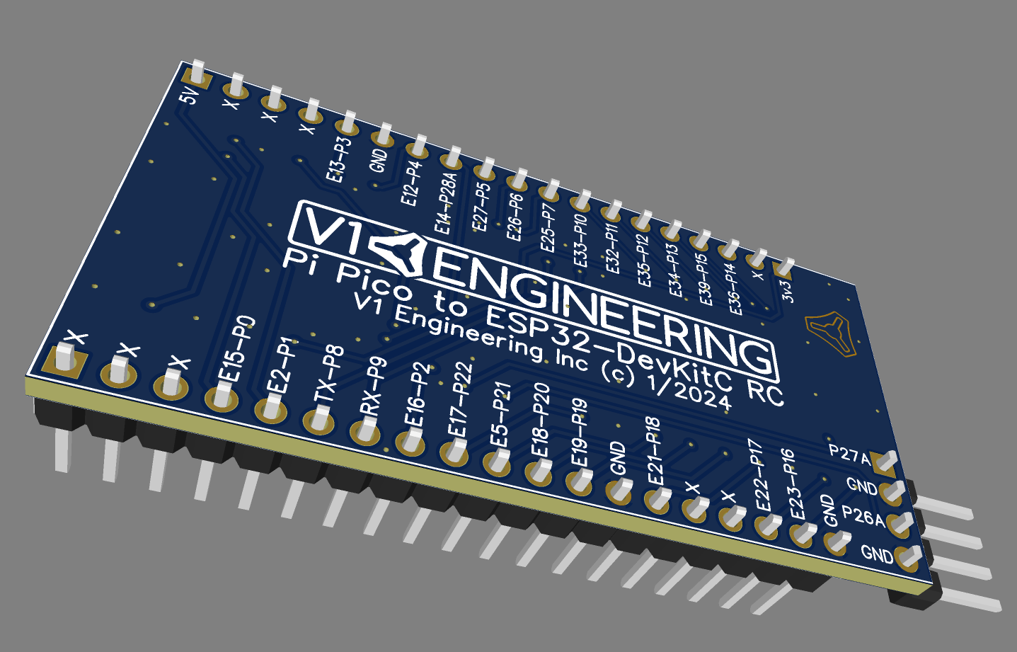
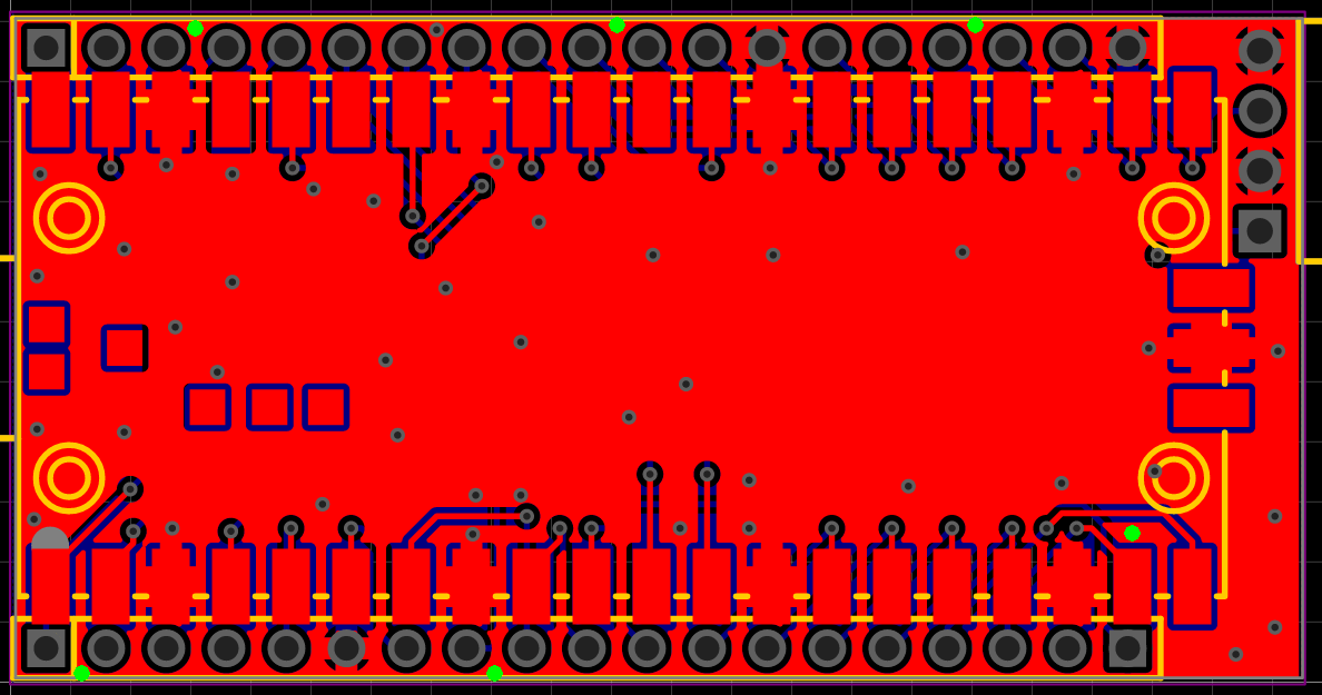
Just finished it. The logos are the same direction as the jackpot.
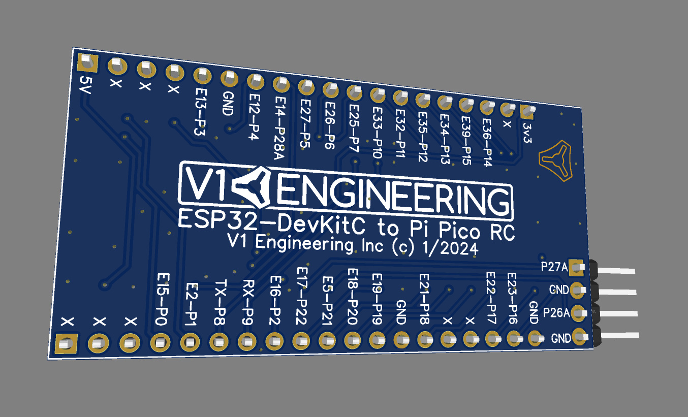
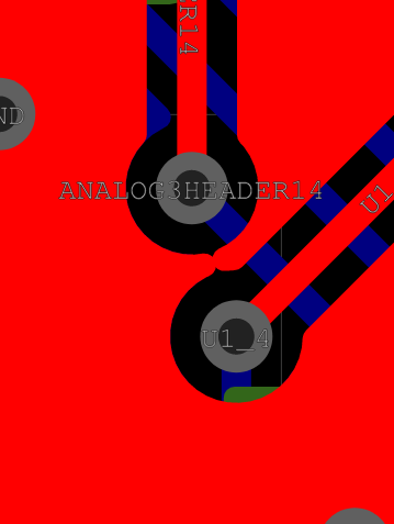
E= esp32 pin P=Pi pico pin.
That way if you look at the jackpot you know what output is what pin, if you use another board it should still work, if not you have the esp io number to reference.
Yeah?
3 Likes
Nice! Taking a look, but mostly following along and learning from others…
Expected “Pi Pico to ESP32 DevKit …” ?
Like the pin remapping labels being visible, and the naming convention.
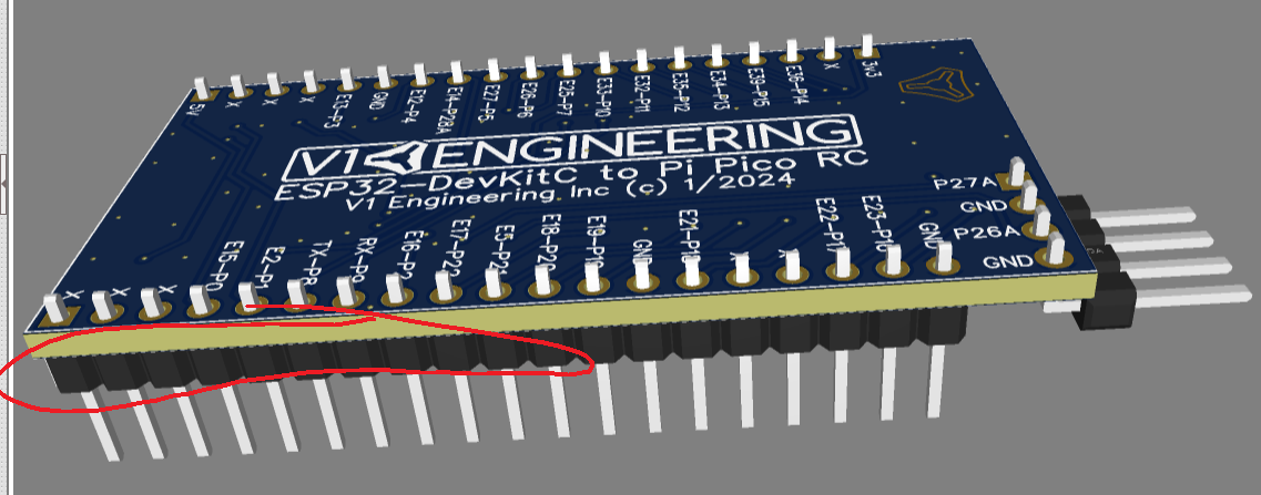
Happy with clearances, and pin lengths/plastic-thickness. given all the components underneath and adjacent header?
Guessing you’re looking for Production version to eventually have RP2040 mounted and heatsinked on top?
EDIT: fwiw eyeballed pinouts…

Is that the correct way? That is easy enough to switch.
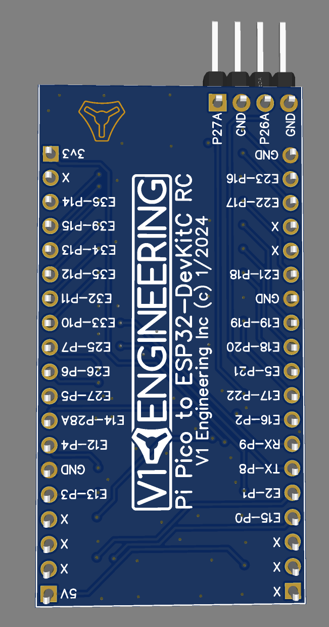
Well looking at your pictures I need to rotate the labels 180 to match the jackpot…
That one on the back is just a place holder. It will either be a 90 header on top or a straight header out of the top. Hand soldered.
nope under, fits snug as a bug in a rug, and I put as much copper as possible on the PCB to heat sink.
What time does the live stream start?? ![]()
![]()
1 Like
Sorry, it is a patreon premium subscription and I see you are only a mere patreon subscriber.
2 Likes
I’ll look at it a bit this weekend.
I’ll buy one to play around with on my test jackpot.
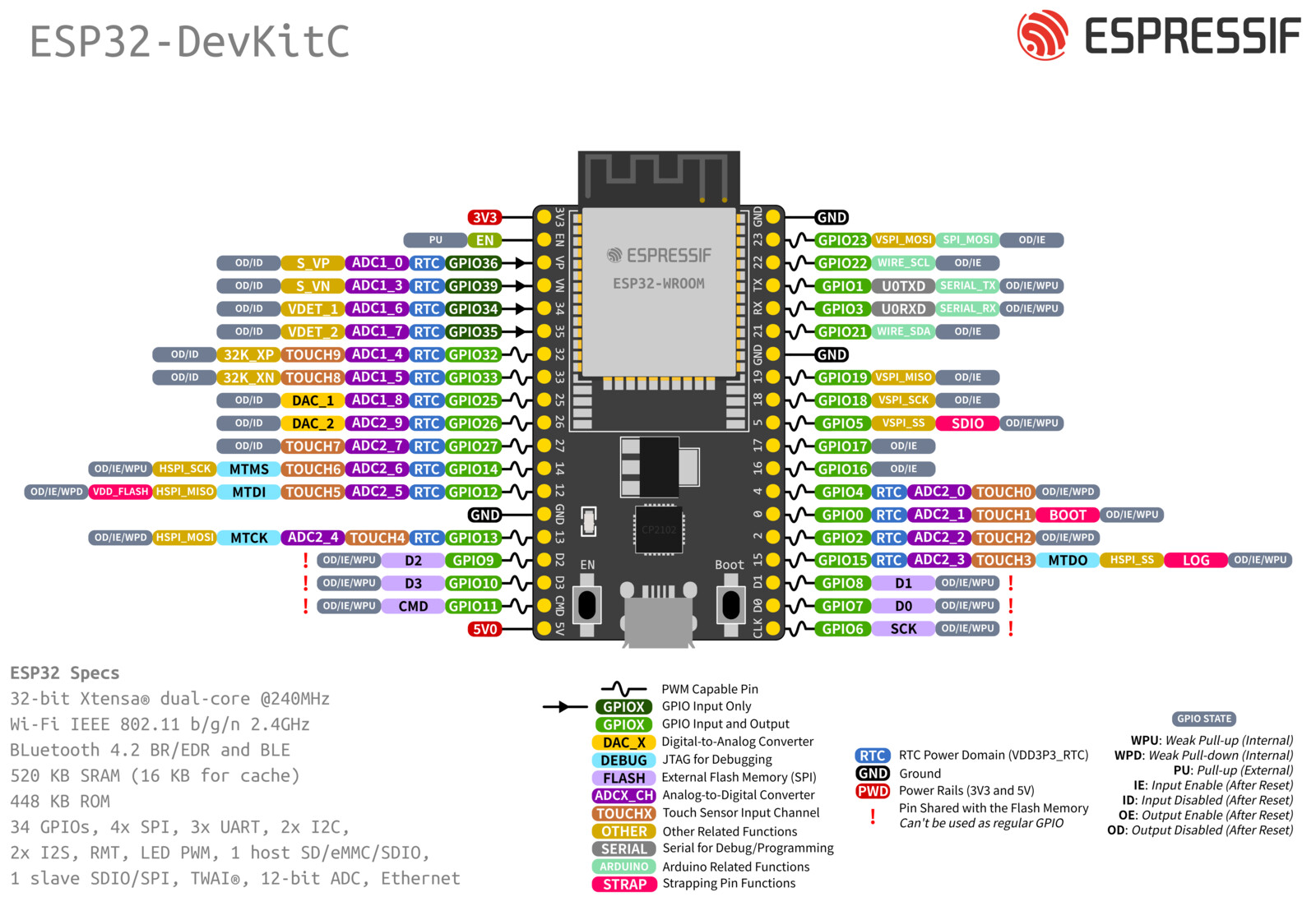
One question- are you using a pico or a pico W? The W wifi may not work well buried on the bottom like that. But I’m not sure the wireless buys much for a Klipper controller anyway.
Pico, we can save a $1-2 not using the wifi version, and we can mount it upside down (hopefully).
2 Likes
LMAO. I pay more than the only pateron he has and I have the printables club too! Dang now he is going to have to get a YouTube membership that we can pay for too LOL
2 Likes
I took a quick glance at the IO routing and it looked OK as a very preliminary first look.
The next step would be to create a table that shows at least the pin name/number on the Pico, the pin number on the header, and the corresponding net name on the Jackpot schematic.
That would help verification, and would also be a starting point for anyone working to implement the required code to use the Bart style TMC interface and GPIO expansion scheme.
1 Like
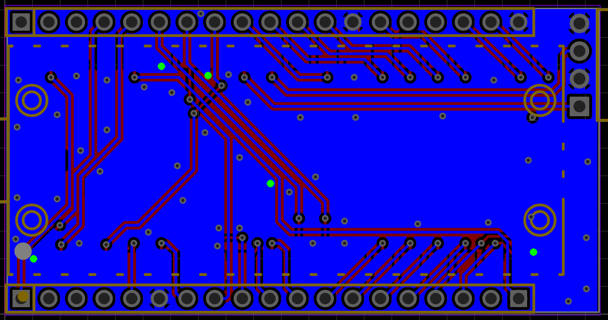
I have the labels on top, beyond that I think it is best to use the Schematic? I can post that link directly. I even have all the pinouts listed with the visuals. Just making a list though, it is very difficult to list each pin’s capabilities and such.
I only used a few net tags for important pins the rest you can highlight the connection and see where it goes.
The esp any pin can pretty much do anything, not the case for the pico.
1 Like
Fwiw - edited my earlier post to add schematic and pinouts to help eyeball everything in one place…
Not a big deal, but are pin mapping labels upside down?
I think with mounting the pico on the bottom that would flop everything side to side if that’s what you are referring to.
1 Like
Perfect thank you.
If you look at the 3D render it should make sense. Designing in a top down see through way is extremely difficult for me so it could be wrong. Let me know if you think it is.
I rotated them so they are the same as the Jackpot.
2 Likes
For situations like that where it’s a ton of lines with basic connections, I really would encourage you to just use netlabels. It’s dramatically less error prone and easier to review.
You also don’t need to use Port symbols, you can just use netlabels. Ports are usually used when going between multiple sheets and where you either want to establish a strict hierarchy (only ports connect between sheets, for instance) or want to just use the ports as a way to signal ‘this is connected to other sheets elsewhere’.
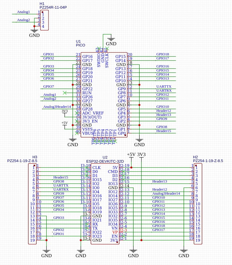
That’s a quick refactoring to show how I’d usually approach something like that. It’s using wires where they make sense (direct links that are ‘pin for pin’) and labels where they make more sense (just linking 2 different pins together without anything ‘interesting’ in the way). I would suggest trying to keep the pin numbers the same so pin 1 goes to pin 1 etc. on H2/H3 and U2. It doesn’t ‘really’ matter in any way for connectors, but it’s just best to keep internal consistency like that where possible.
Layout:
I’d still dial back the thickness on the thermal reliefs for the ground. I’d make them 0.25mm or something like that. As it is, they’re not really thermal reliefs at all because there’s so much copper. You don’t need to make them huge because each one has 4 spokes (so 0.25mm routing width means 1mm total) and they’re so short that they have essentially zero effect on resistance/inductance.
That’s getting a little marginal, I’d move one of the vias so that’s a more ‘solid’ connection.
Same thing with the thermal reliefs on the SMD pads. I’d lower the thickness or just commit and do a full pour-over. I often end up doing full pour-over on SMT pads that connect to planes because if it’s being reflowed then it doesn’t need a thermal relief, all the copper should be the same temperature. Thermal reliefs are really for hand soldering purposes and maybe arguably less important for wave or selective soldering. If you’re doing it by hand, a decent iron and taking a little more time on those joints gets the job done just as well.
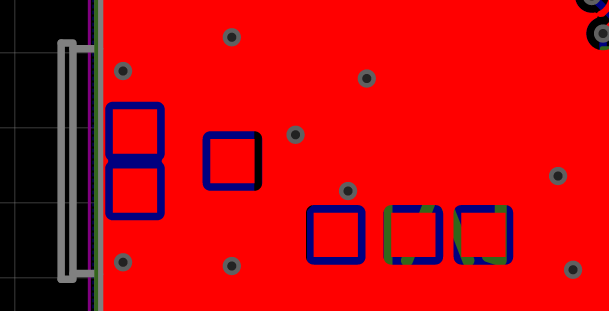
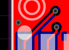
If you’re not using these, I’d just remove them entirely or at least edit them so that they don’t have any paste or have solder mask above them. I’d also move any vias away that are too close. Castellated boards typically sit directly flat on top of the PCB they’re on so that has a chance of pressing any solder paste out sideways and creating connections where you don’t want them. There doesn’t appear to be any reason to solder those test points to the board.
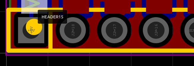
The board house will probably sort this for you, but in general it’s best practice to not have any silk screening over pads where possible. Best case, nothing happens. Worst case, you have silk screen fragments on your pads that can interfere with soldering. I would manually edit this footprint and either remove the silkscreen entirely, because it really isn’t doing anything useful, or just remove that one line that interferes. As for the pin1 component mark, I’d delete it if you don’t need it (because it won’t exist there anyway) or move it somewhere, even if that’s in-board and not visible once the part is placed.
That’s a good general note about polarity markings: They should, where possible, be visible with the component installed so that you can inspect the components post-assembly for correct orientation. This is a much more common failure mode than you might expect. If they can’t be placed somewhere visible in the final assembly, placing them somewhere on the board where they can’t be seen and then checking the assembled boards vs a printout or bare board can work as a backup plan.
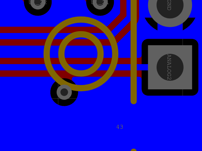
Random disconnected via
I’d still throw a few more vias around:
Or at least somewhat close to those locations. This is very much a ‘just because I can’ approach, not actually needed because the top side is so complete.
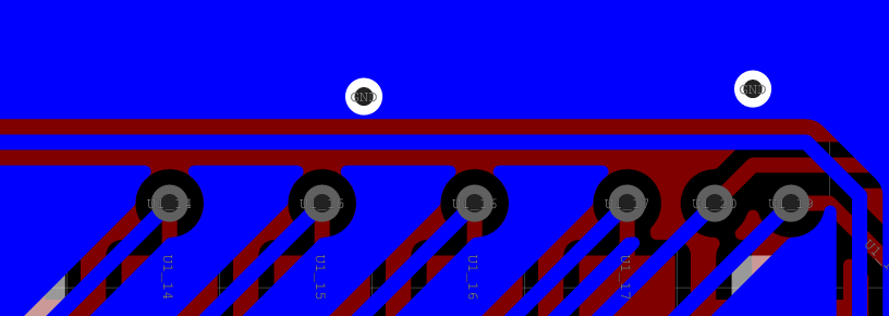
Any time you see something like this, consider if you can move a trace slightly and have the plane link back up:
I’d also try to move the via in the bottom right to make that copper connection stronger.
Same thing here: Moving that trace up a little and then adding a few vias along the bottom side of the trace.
Other than that, looks good. I haven’t checked for pinouts or correct circuit connections because I’m not as familiar with what’s going on at that level of the design and seems like a few people have already cracked into it.
1 Like
I love that! I was having an issue trying to keep upside down and flipped right so I was actually using the lines to visualize it…seeing how it flipped open, top to bottom. I absolutely do not mind changing it now. I just needed to see where each one went and was flipping between views to try an minimize crossing the plane.
I had no idea about net labels and port labels, I can change that.
The headers were actually an afterthought I literally just dropped them on. I forgot all about them until the silkscreen started to get added.
I am sorry, I know that must be the most hideous thing you have seen!! ![]()
I can not find a way to change that. I can do solid or spokes, only options.
K -done
Finally figured out how to do that.
I can try again, There has to be a way to edit these. GOt it…Done. Thank you, I knew that seemed bad.
I will remove it.
Now that I know how to do that, no problem!
got it
Gotcha
done, missed that one for sure.
HAHAHAH maybe a little better than last time, but ummmm, not by much.
Thank you for looking at it. I feel a bit better buying a couple now.
3 Likes