Hello! That’s a great project, and a perfect first step into PCB design.
Creating a PCB design calls for Electronic Design Automation (EDA) software (like KiCad, EasyEDA, or Eagle) needed to create the Gerber files that PCBWay requires for manufacturing.
I can provide the exact schematic (the “blueprint”) for what you want to do and, more importantly, guide you on the different paths you can take to get this made, even with zero experience.
 The Circuit Schematic You Need
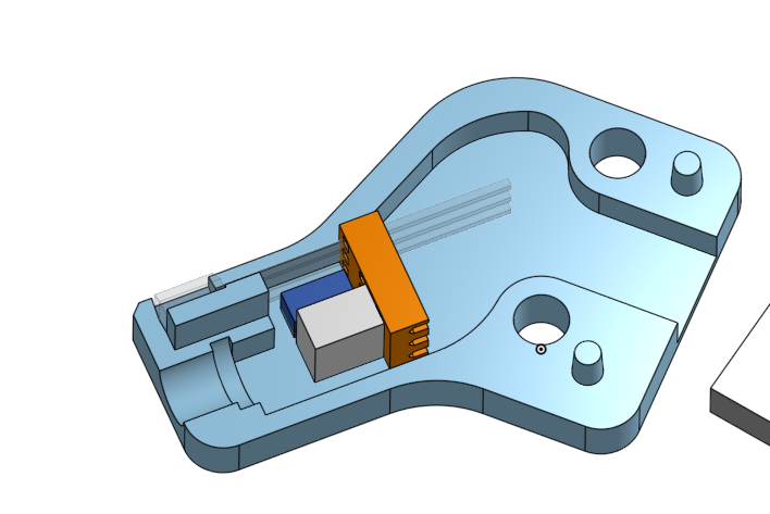
You are correct about all the components. Your AH3391Q sensor has an “open-drain” output. This means it can pull the signal line to Ground (LOW) when a magnet is present, but it cannot push the line to VCC (HIGH). It just “lets go” of the line.
That’s why the 1kΩ pull-up resistor is essential. It connects the signal line to your power source (e.g., 5V), holding it HIGH by default. When the sensor triggers, it overpowers the resistor and pulls the line LOW.
Here is the complete circuit schematic, including your bi-color LED idea (which I’ve simplified to two separate LEDs for clarity, as it’s much easier to wire).
Components:
- U1: Your
AH3391Q-P-B Hall effect sensor
- R1:
1kΩ Resistor (This is the pull-up resistor)
- C1:
100nF (or 0.1µF) Capacitor (This is the filter/decoupling capacitor)
- LED1 (Green): A standard 3mm or 5mm green LED (your “operational” light)
- R2 (for LED1):
1kΩ Resistor (This is a current-limiter for the green LED)
- LED2 (Red): A standard 3mm or 5mm red LED (your “triggered” light)
- R3 (for LED2):
1kΩ Resistor (This is a current-limiter for the red LED)
- J1: A 3-pin header (to connect VCC, GND, and Signal to your CNC controller)
Connections:
Your board will have 3 main lines, or “rails,” coming from the 3-pin header J1:
- VCC (Your controller’s +5V or +3.3V line)
- GND (The controller’s Ground line)
- SIG (The Signal line to the controller’s endstop pin)
Here is how everything connects:
- Sensor (U1):
- Pin 1 (VDD) → VCC
- Pin 2 (GND) → GND
- Pin 3 (OUT) → SIG
- Filter Cap (C1): Connects between VCC and GND (place it physically close to the sensor’s Pin 1 and 2).
- Pull-up Resistor (R1): Connects between VCC and SIG.
- “Operational” LED (Green):
R2 connects from VCC to the Anode (+) of LED1.- The Cathode (-) of
LED1 connects to GND.
- (This LED will be on whenever the board has power.)
- “Triggered” LED (Red):
R3 connects from VCC to the Anode (+) of LED2.- The Cathode (-) of
LED2 connects to SIG.
- (This is the clever part: When the sensor is not triggered,
SIG is HIGH, so both sides of the red LED are at VCC and it stays OFF. When the sensor is triggered, it pulls SIG to GND, allowing current to flow and turning the red LED ON.)
 How to Get This Made (3 Paths)
Since you have no PCB experience, here are your options from easiest to hardest.
Option 1: The “Shortcut” (Easiest)
This circuit is a very common solution. Many people in the V1E, Voron, and general 3D printing/CNC communities have already designed this exact PCB and shared their files.
- Go to GitHub, OSHWLab (EasyEDA’s community), or Thingiverse.
- Search for “hall effect endstop pcb,” “v1e hall effect,” or “voron hall effect endstop.”
- You will likely find a project that includes a
.zip file of the Gerber files.
- You can download that
.zip file and upload it directly to PCBWay or JLCPCB for ordering. You don’t have to design anything.
Option 2: The “DIY / Learning” (Recommended First Step)
Before you spend money on a 1-month wait for PCBs, try building one right now. Buy a small piece of protoboard (or “perfboard”).
A perfboard is a simple grid of holes with copper pads. You place your Through-Hole components (your sensor, resistors, and LEDs are all through-hole) into the holes and connect them by soldering their legs together or using small jumper wires on the underside.
This will cost you about $2, take 30 minutes, and teach you the basics of soldering and how the circuit works.
Option 3: The “Full Design” (The Big Leap)
If you are set on designing your own PCB, this is the path.
- Get Software: Download a free, popular EDA program. EasyEDA is a great choice for beginners because it’s web-based and fully integrated with a component supplier (LCSC) and a PCB manufacturer (JLCPCB). KiCad is the open-source, professional-grade standard.
- Draw the Schematic: In the software, you’ll first re-create the schematic I described above. You’ll place the symbols for the resistor, capacitor, etc., and draw “nets” (wires) to connect them.
- Design the PCB Layout: You’ll switch to the layout editor. Here, you will:
- Draw the physical shape of your board.
- Place the footprints (the physical pads/holes) for each component.
- Run “traces” (the copper lines) to connect the footprints as defined in your schematic.
- Export Gerber Files: Once you’re done, you’ll click “Export” → “Gerber”. This will package all the manufacturing files (for copper layers, drill holes, and silk-screen text) into a single
.zip file.
- Order: You will upload this
.zip file to PCBWay’s website, choose your color (usually green), and place your order.
This is a fantastic learning journey, but it will take a few nights of watching YouTube tutorials to get the hang of it.
My advice? Start with Option 2 (Perfboard). If you like it and it works, and you then decide you want to make 10 more that look cleaner, then you can move on to Option 3 (Learn EasyEDA) or just take Option 1 (Download Gerbers).
Would you like me to help you find a pre-made, open-source Gerber file for this circuit?